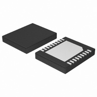
NCP5220MNR2G ON Semiconductor, NCP5220MNR2G Datasheet - Page 4

NCP5220MNR2G
Manufacturer Part Number
NCP5220MNR2G
Description
IC CTLR PWM DUAL BUCK PWR 20-DFN
Manufacturer
ON Semiconductor
Datasheet
1.NCP5220MNR2G.pdf
(18 pages)
Specifications of NCP5220MNR2G
Applications
Controller, DDR
Voltage - Input
5 ~ 12 V
Number Of Outputs
2
Operating Temperature
0°C ~ 70°C
Mounting Type
Surface Mount
Package / Case
20-TFDFN
Switching Frequency
250 KHz
Operating Temperature Range
0 C to + 70 C
Mounting Style
SMD/SMT
Duty Cycle (max)
100%
Lead Free Status / RoHS Status
Lead free / RoHS Compliant
Voltage - Output
-
Lead Free Status / Rohs Status
Lead free / RoHS Compliant
Other names
NCP5220MNR2G
NCP5220MNR2GOSTR
NCP5220MNR2GOSTR
Available stocks
Company
Part Number
Manufacturer
Quantity
Price
Company:
Part Number:
NCP5220MNR2G
Manufacturer:
SIPEX
Quantity:
4 100
Maximum ratings are those values beyond which device damage can occur. Maximum ratings applied to the device are individual stress limit
values (not normal operating conditions) and are not valid simultaneously. If these limits are exceeded, device functional operation is not implied,
damage may occur and reliability may be affected.
1. This device series contains ESD protection and exceeds the following tests: Human Body Model (HBM) " 2.0 kV per JEDEC standard:
2. Latchup Current Maximum Rating: " 150 mA per JEDEC standard: JESD78.
PIN DESCRIPTION
MAXIMUM RATINGS
Power Supply Voltage (Pin 16) to AGND (Pin 7)
BOOT (Pin 17) to AGND (Pin 7)
Gate Drive (Pins 12, 13, 18, 19) to AGND (Pin 7)
Input / Output Pins to AGND (Pin 7)
Pins 1−3, 5, 6, 8−10, 14−15, 20
PGND (Pin 4), GND_1P5 (Pin 11) to AGND (Pin 7)
Thermal Characteristics
Operating Junction Temperature Range
Operating Ambient Temperature Range
Storage Temperature Range
Moisture Sensitivity Level
Pin
10
11
12
13
14
15
16
17
18
19
20
21
JESD22–A114. Machine Model (MM) " 200 V per JEDEC standard: JESD22–A115.
DFN−20 Plastic Package
Thermal Resistance Junction−to−Air
1
2
3
4
5
6
7
8
9
COMP_1P5
GND_1P5
SW_DDQ
BG_DDQ
TG_DDQ
BG_1P5
5VDUAL
TH_PAD
Symbol
SLP_S5
TG_1P5
SLP_S3
FBDDQ
FBVTT
FB1P5
COMP
PGND
VDDQ
AGND
BOOT
VTT
SS
VDDQ error amplifier compensation node.
DDQ regulator feedback pin.
Soft−start pin of DDQ and MCH.
Power ground.
VTT regulator output.
Power input for VTT linear regulator.
Analog ground connection and remote ground sense.
VTT regulator pin for closed loop regulation.
Active LOW control signal to activate S5 Power OFF State.
V1P5 switching regulator feedback pin.
Power ground for V1P5 regulator.
Gate driver output for V1P5 regulator low side N−Channel Power FET.
Gate driver output for V1P5 regulator high side N−Channel Power FET.
Active LOW control signal to activate S3 sleep state.
V1P5 error amplifier compensation node.
5.0 V dual supply input, which is monitored by undervoltage lock out circuitry.
Gate driver input supply, which is monitored by undervoltage lock out circuitry, and a boost capacitor
connection between SWDDQ and this pin.
Gate driver output for DDQ regulator high side N−Channel Power FET.
Gate driver output for DDQ regulator low side N−Channel Power FET.
DDQ regulator switch node and current limit sense input.
Copper pad on bottom of IC used for heatsinking. This pin should be connected to the ground plane under
the IC.
Rating
http://onsemi.com
NCP5220
4
Description
5VDUAL
Symbol
BOOT
V
R
MSL
T
V
Vg
GND
T
T
qJA
stg
IO
A
J
−4.0 for t100 ns; 14
− 55 to +150
0 to + 150
−0.3, 6.0
−0.3 DC,
−0.3, 6.0
−0.3, 0.3
0 to + 70
−0.3, 14
Value
2.0
35
°C/W
Unit
°C
°C
°C
V
V
V
V
V


