ISL62884CIRTZ Intersil, ISL62884CIRTZ Datasheet - Page 21

ISL62884CIRTZ
Manufacturer Part Number
ISL62884CIRTZ
Description
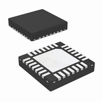
IC REG PWM SGL PHASE 28TQFN
Manufacturer
Intersil
Datasheet
1.ISL62884CHRTZ.pdf
(30 pages)
Specifications of ISL62884CIRTZ
Applications
Controller, Intel IMVP-6
Voltage - Input
4.5 ~ 25 V
Number Of Outputs
1
Voltage - Output
0.0125 ~ 1.5 V
Operating Temperature
-40°C ~ 100°C
Mounting Type
Surface Mount
Package / Case
28-VQFN
Lead Free Status / RoHS Status
Lead free / RoHS Compliant
Available stocks
Company
Part Number
Manufacturer
Quantity
Price
Part Number:
ISL62884CIRTZ
Manufacturer:
NA
Quantity:
20 000
Optional Slew Rate Compensation Circuit
For 1-Tick VID Transition
During a large VID transition, the DAC steps through the
VIDs at a controlled slew rate, such as 1.25µs per tick
(12.5mV), controlling output voltage V
10mV/µs.
FIGURE 20. OPTIONAL SLEW RATE COMPENSATION
FIGURE 19. LOOP GAIN T2(s) MEASUREMENT SET-UP
V
IN
Idroop_vid
COMP
VID<0:6>
LOOP GAIN =
DRIVER
Vcore
GATE
Q1
INTERNAL TO
Ivid
Vfb
CIRCUIT FOR1-TICK VID TRANSITION
E/A
MOD
Q2
IC
CHANNEL B
CHANNEL A
COMP
FB
LOAD LINE SLOPE
Σ
ANALYZER
CHANNEL A
NETWORK
Idroop_vid
EA
L
VDAC
+
21
-
VID
C
R
Rdroop
OUT
vid
DAC
I
X 1
vid
EXCITATION OUTPUT
C
V
vid
O
+
+
RTN
I
VIDs
VSS
20
O
core
Ω
OPTIONAL
Vcore
VID<0:6>
slew rate at
VSS
ISOLATION
TRANSFORMER
SENSE
CHANNEL B
ISL62884C
Figure 20 shows the waveforms of 1-tick VID transition.
During 1-tick VID transition, the DAC output changes at
approximately 15mV/µs slew rate, but the DAC cannot
step through multiple VIDs to control the slew rate.
Instead, the control loop response speed determines
V
voltage slew rate. However, the controller senses the
inductor current increase during the up transition, as the
I
voltage V
Similar behavior occurs during the down transition.
To control V
one can add the R
cancels I
When V
induced I
where C
In the meantime, the R
domain expression is shown in Equation 27:
It is desired to let I
are Equation 28:
and Equation 29:
The result is Equation 30:
and Equation 31:
For example: given LL = 5.7mΩ, R
C
dV
and Equation 31 gives C
It’s recommended to select the calculated R
start with the calculated C
actual board to get the best performance.
During normal transient response, the FB pin voltage is
held constant, therefore is virtual ground in small signal
sense. The R
ground and the real ground, and hence has no effect on
transient response.
C
I
C
R
R
I
droop_vid
droop
vid
core
out
vid
vid
vid
vid
fb
t ( )
×
×
/dt = 15mV/µs, Equation 30 gives R
=
=
= 410µF, dV
slew rate. Ideally, V
t ( )
dV
------------
C
=
C
------------------------- -
R
dt
vid
core
R
out
out
droop
C
fb
droop_vid
=
droop
core
droop
vid
waveform shows, and will droop the output
C
------------------------- -
=
=
×
core
R
is the total output capacitance.
increases, the time domain expression of the
out
×
C
LL
vid
C
------------------------- -
droop
accordingly, making V
R
dV
------------
out
out
change is as shown in Equation 26:
×
dt
droop
×
-C
slew rate during 1-tick VID transition,
LL
fb
------------------ -
×
dV
------------------ -
×
.
vid
dV
------------
vid
core
LL
×
LL
dt
dt
vid
×
core
⎛
⎜
⎜
⎝
fb
-C
dV
------------------ -
1 e
network is between the virtual
×
(t) cancel I
/dt = 10mV/µs and
–
dt
dV
------------------ -
vid
core
vid
------------------------------- -
R
dt
core
core
vid
-C
vid
vid
branch, whose current I
×
vid
t –
⎛
⎜
⎜
⎝
×
= 2730pF.
1 e
value and tweak it on the
will follow the FB pin
C
–
vid
branch current I
droop_vid
-------------------------- -
C
⎞
⎟
⎟
⎠
out
core
t –
droop
×
LL
slew rate slow.
⎞
⎟
⎟
⎠
(t). So there
= 0.57kΩ,
vid
vid
March 16, 2010
= 0.57kΩ
value and
vid
(EQ. 26)
(EQ. 27)
(EQ. 28)
(EQ. 29)
(EQ. 30)
(EQ. 31)
FN7591.0
vid
time


