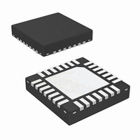
ISL62884CIRTZ Intersil, ISL62884CIRTZ Datasheet - Page 20

ISL62884CIRTZ
Manufacturer Part Number
ISL62884CIRTZ
Description
IC REG PWM SGL PHASE 28TQFN
Manufacturer
Intersil
Datasheet
1.ISL62884CHRTZ.pdf
(30 pages)
Specifications of ISL62884CIRTZ
Applications
Controller, Intel IMVP-6
Voltage - Input
4.5 ~ 25 V
Number Of Outputs
1
Voltage - Output
0.0125 ~ 1.5 V
Operating Temperature
-40°C ~ 100°C
Mounting Type
Surface Mount
Package / Case
28-VQFN
Lead Free Status / RoHS Status
Lead free / RoHS Compliant
Available stocks
Company
Part Number
Manufacturer
Quantity
Price
Part Number:
ISL62884CIRTZ
Manufacturer:
NA
Quantity:
20 000
Substitution of Equation 19 into Equation 1 gives
Equation 20:
Therefore:
Substitution of Equation 21 and application of the OCP
condition in Equation 17 gives Equation 22:
where I
corresponding droop current. For example, given
R
Equation 22 gives R
A resistor from COMP to GND can adjust the internal OCP
threshold, providing another dimension of fine-tune
flexibility. Table 3 shows the detail. It is recommended to
scale I
approximately the desired OCP level, then use R
fine tune the OCP level if necessary.
Load Line Slope
Refer to Figure 9.
For inductor DCR sensing, substitution of Equation 16
into Equation 2 gives the load line slope expression in
Equation 23.
For resistor sensing, substitution of Equation 20 into
Equation 2 gives the load line slope expression in
Equation 24:
Substitution of Equation 17 and rewriting Equation 23,
or substitution of Equation 21 and rewriting Equation 24
gives the same result in Equation 25:
One can use the full load condition to calculate R
For example, given I
LL = 5.7mΩ, Equation 25 gives R
It is recommended to start with the R
calculated by Equation 25, and fine tune it on the actual
board to get accurate load line slope. One should record
the output voltage readings at no load and at full load for
load line slope calculation. Reading the output voltage at
lighter load instead of full load will increase the
measurement error.
Compensator
Figure 11 shows the desired load transient response
waveforms. Figure 17 shows the equivalent circuit of a
voltage regulator (VR) with the droop function. A VR is
R
R
LL
LL
I
R
droop
sen
droop
i
i
=
=
=
=
= 1mΩ, I
2R
--------------------------- -
2R
---------------------------------------
V
------------------ -
V
------------------ -
droop
=
I
droop
droop
I
=
droop
sen
droopmax
omax
I
I
sen
o
o
---- -
R
2
----------------
I
droop
i
×
×
I
×
o
R
I
such that the default OCP threshold gives
=
=
I
o
omax
is the full load current, I
sen
omax
2R
---------------------- -
2R
------------------------------------------ -
×
LL
droop
sen
×
R
I
i
o
= 5A and I
i
×
R
omax
= 200Ω.
i
R
×
droop
----------------------------------------- -
R
ntcnet
20
= 5A, I
R
ntcnet
+
droopmax
R
droop
sum
droopmax
×
droopmax
droop
DCR
= 0.57kΩ.
= 50µA,
= 50µA and
value
is the
droop
comp
(EQ. 20)
(EQ. 21)
(EQ. 22)
(EQ. 23)
(EQ. 24)
(EQ. 25)
ISL62884C
.
to
equivalent to a voltage source (= VID) and output
impedance Z
slope LL, i.e., constant output impedance in the entire
frequency range, V
has a square change.
A VR with active droop function is a dual-loop system
consisting of a voltage loop and a droop loop which is a
current loop. However, neither loop alone is sufficient to
describe the entire system. The spreadsheet (see
Figure 21) shows two loop gain transfer functions, T1(s)
and T2(s), that describe the entire system. Figure 18
conceptually shows T1(s) measurement set-up and
Figure 19 conceptually shows T2(s) measurement
set-up. The VR senses the inductor current, multiplies it
by a gain of the load line slope, then adds it on top of the
sensed output voltage and feeds it to the compensator.
T(1) is measured after the summing node, and T2(s) is
measured in the voltage loop before the summing node.
The spreadsheet (see Figure 21) gives both T1(s) and
T2(s) plots. However, only T2(s) can be actually
measured on an ISL62884C regulator.
T1(s) is the total loop gain of the voltage loop and the
droop loop. It always has a higher crossover frequency
than T2(s) and has more meaning of system stability.
T2(s) is the voltage loop gain with closed droop loop. It
has more meaning of output voltage response.
Design the compensator to get stable T1(s) and T2(s)
with sufficient phase margin, and output impedance
equal or smaller than the load line slope.
FIGURE 17. VOLTAGE REGULATOR EQUIVALENT
FIGURE 18. LOOP GAIN T1(s) MEASUREMENT SET-UP
V
IN
LOOP GAIN =
DRIVER
VID
GATE
Q1
out
CIRCUIT
MOD
(s). If Z
Q2
CHANNEL B
CHANNEL A
CHANNEL A
ANALYZER
NETWORK
o
Z
COMP
out(s)
will have square response when I
out
= LL
LOAD LINE SLOPE
EA
L
VR
(s) is equal to the load line
+
-
VID
EXCITATION OUTPUT
C
OUT
i
O
V
20
LOAD
O
Ω
I
O
+
+
V
+
ISOLATION
TRANSFORMER
-
O
CHANNEL B
March 16, 2010
FN7591.0
o


