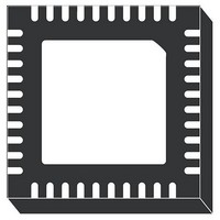
L6756D STMicroelectronics, L6756D Datasheet - Page 22

L6756D
Manufacturer Part Number
L6756D
Description
IC CTLR 2/3/4PH BUCK 40-VFQFPN
Manufacturer
STMicroelectronics
Datasheet
1.L6756DTR.pdf
(36 pages)
Specifications of L6756D
Applications
Controller, Intel VR10, VR11, VR11.1
Voltage - Input
12V
Number Of Outputs
4
Voltage - Output
0.3 ~ 1.6 V
Operating Temperature
0°C ~ 70°C
Mounting Type
Surface Mount
Package / Case
40-VFQFN, 40-VFQFPN
Output Voltage
3 V
Input Voltage
- 0.3 V to + 15 V
Switching Frequency
185 KHz to 215 KHz
Operating Temperature Range
- 40 C to + 150 C
Mounting Style
SMD/SMT
Lead Free Status / RoHS Status
Lead free / RoHS Compliant
Available stocks
Company
Part Number
Manufacturer
Quantity
Price
Output voltage positioning
5.3
Note:
5.4
Caution:
Note:
22/36
Output voltage load-line definition
L6756D is able to introduce a dependence of the output voltage on the load current
recovering part of the drop due to the output capacitor ESR in the load transient. Introducing
a dependence of the output voltage on the load current, a static error, proportional to the
output current, causes the output voltage to vary according to the sensed current.
Figure 7
flowing across the inductor(s) is read through the R - C filter across CSx and CSxN pins. R
programs a transconductance gain and generates a current I
of the phase x. The sum of the I
gives the final gain to program the desired load-line slope
Time constant matching between the inductor (L / DCR) and the current reading filter (RC)
is required to implement a real equivalent output impedance of the system so avoiding over
and/or under shoot of the output voltage as a consequence of a load transient. The output
characteristic vs. load current is then given by (Offset disabled):
Where R
power supply can be then represented by a “real” voltage generator with an equivalent
output resistance R
R
Load-Line (DROOP) implementation is optional, in case it is not desired, the resulting
current information available on VDRP may be employed for other purposes, such as an
additional Load Indicator (LI2). In this case, simply connect a resistor R
resulting voltage drop across R
the following relationship:
In case no additional information about the delivered current is requested, the VDRP pin can
be shorted to SGND.
Output voltage offset
The current (I
output voltage by connecting a resistor R
rent generates a voltage drop according to the connected R
grammed as follow:
Offset resistor impacts the voltage positioning! It need to be considered in series to R
Offset implementation is optional: in case it is not desired, simply consider using R
V
R
V
V
OUT
FB
LI2
CORE
FB
resistor can be then designed according to the R
=
=
=
R
R
=
VID R
LL
LI2
shows the current sense circuit used to implement the load-line. The current
LL
VID
⋅
is the resulting load-line resistance implemented by the controller. The whole
⋅
------------ -
DCR
–
DCR
------------ - I
R
OS
R
–
G
G
(
FB
) sunk from the VSEN pin allows programming a positive offset (V
R
FB
⋅
⋅
I
LL
OUT
DROOP
+
and a voltage value of VID.
R
OS
) I
=
⋅
DROOP
VID R
LI2
CSx
–
will be proportional to the delivered current according to
current is then sourced by the VFB pin (I
+
FB
R
OS
⋅
DCR
------------ - I
OS
R
⋅
G
I
OS
to V
⋅
OUT
OUT
=
in series to the FB loop. The sunk cur-
LL
VID R
specifications as follow:
(Figure
–
OS
CSx
LL
. Output voltage is then pro-
⋅
I
proportional to the current
OUT
6).
LI2
to SGND: the
DROOP
OS
OS
). R
) for the
L6756D
FB
= 0
FB
.
Ω
G
.


