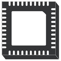
L6756D STMicroelectronics, L6756D Datasheet - Page 10

L6756D
Manufacturer Part Number
L6756D
Description
IC CTLR 2/3/4PH BUCK 40-VFQFPN
Manufacturer
STMicroelectronics
Datasheet
1.L6756DTR.pdf
(36 pages)
Specifications of L6756D
Applications
Controller, Intel VR10, VR11, VR11.1
Voltage - Input
12V
Number Of Outputs
4
Voltage - Output
0.3 ~ 1.6 V
Operating Temperature
0°C ~ 70°C
Mounting Type
Surface Mount
Package / Case
40-VFQFN, 40-VFQFPN
Output Voltage
3 V
Input Voltage
- 0.3 V to + 15 V
Switching Frequency
185 KHz to 215 KHz
Operating Temperature Range
- 40 C to + 150 C
Mounting Style
SMD/SMT
Lead Free Status / RoHS Status
Lead free / RoHS Compliant
Available stocks
Company
Part Number
Manufacturer
Quantity
Price
Pins description and connection diagrams
10/36
Table 2.
30 to
Pin#
28
29
33
34
35
36
37
38
39
40
Thermal pad
LTB_GAIN
G1 to G4
VR_RDY
DRVON
PSI_A
Name
VREF
IMON
GND
VCC
CS4
Pin description (continued)
Channel 4 current sense positive input. Connect through an R-C filter to the
phase-side of the channel 4 inductor. When working at 2 or 3 phase, short to
the regulated voltage.
External driver enable. CMOS output used to control the external driver status:
pulled-low to manage HiZ conditions or pulled-high for normal driver switching.
PWM outputs. Connect to external drivers PWM inputs. The device is able to
manage HiZ status by setting the pins floating.
By shorting to GND G4 or G2 and G4, it is possible to program the device to
work at 3 or 2 phase respectively.
This pin provide a 2.5 V reference. Filter with 1 nF (max) to SGND.
All the internal references are referred to this pin. Connect to the PCB signal
ground.
Device power supply.
Operative voltage is 12 V ±15 %. Filter with at least 1 μF MLCC vs. ground.
Open drain output set free after SS has finished and pulled low when triggering
any protection. Pull up to a voltage lower than 3.3 V (typ), if not used it can be
left floating.
Load transient boost technology
PSI action configuration pin.
This pins configures the functionality of the PSI# / VR10 pin according to
Table 9
VR10: Short to SGND to configure the VID_SEL functionality. The controller
will not manage low power-states but will be backward compatible with VR10 /
VR11 platforms.
PSI#: The device will work in VR11 mode and perform low power-states
management through the PSI# pin. See
Current monitor output. A current proportional to the read current is sourced
from this pin. Connect through a resistor R
indicator. Connect the load indicator directly to VR11.1 CPUs.The pin voltage
is clamped to 1.1V max to preserve the CPU from excessive voltages.
Thermal pad connects the silicon substrate and makes good thermal contact
with the PCB. Connect to the PGND plane.
as follow:
®
gain pin. See
Function
Section 7
MON
to FBG to implement a load
Section 9.2
for details.
for details.
L6756D


