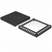
ISL8103IRZ Intersil, ISL8103IRZ Datasheet - Page 11

ISL8103IRZ
Manufacturer Part Number
ISL8103IRZ
Description
IC CTRLR PWM BUCK 3PHASE 40-QFN
Manufacturer
Intersil
Datasheet
1.ISL8103IRZ-T.pdf
(28 pages)
Specifications of ISL8103IRZ
Pwm Type
Voltage Mode
Number Of Outputs
1
Frequency - Max
1.5MHz
Duty Cycle
66.6%
Voltage - Supply
4.75 V ~ 12.6 V
Buck
Yes
Boost
No
Flyback
No
Inverting
No
Doubler
No
Divider
No
Cuk
No
Isolated
No
Operating Temperature
-40°C ~ 85°C
Package / Case
40-VFQFN, 40-VFQFPN
Frequency-max
1.5MHz
Lead Free Status / RoHS Status
Lead free / RoHS Compliant
Current Sampling
In order to realize proper current balance, the currents in
each channel must be sampled every switching cycle. This
sampling occurs during the forced off-time, following a PWM
transition low. During this time the current sense amplifier
uses the ISEN inputs to reproduce a signal proportional to
the inductor current, I
a scaled version of the inductor current. The sample window
opens exactly 1/6 of the switching period, t
PWM transitions low. The sample window then stays open
the rest of the switching cycle until PWM transitions high
again, as illustrated in Figure 4.
The sampled current, at the end of the t
proportional to the inductor current and is held until the next
switching period sample. The sampled current is used only
for channel current balance.
The ISL8103 supports MOSFET r
sample each channel’s current for channel current balance.
The internal circuitry, shown in Figure 5 represents Channel
N of an N-channel converter. This circuitry is repeated for
NOTE: Channel 2 and 3 are optional.
FIGURE 3. CHANNEL 1 PWM FUNCTION AND CURRENT-
V
COMP
FILTER
FIGURE 4. SAMPLE AND HOLD TIMING
BALANCE ADJUSTMENT
OLD SAMPLE
CURRENT
+
I
ER
-
+
f(s)
I
1
PWM
L
-
. This sensed current, I
I
AVG
SAWTOOTH SIGNAL
SWITCHING PERIOD
SAMPLING PERIOD
11
÷ N
I
L
TIME
DS(ON)
+
I
-
SEN
PWM1
SAMPLE
Σ
current sensing to
SW
SEN
, after the
NEW SAMPLE
CURRENT
, is
CONTROL
TO GATE
, is simply
LOGIC
I
I
2
3
ISL8103
each channel in the converter, but may not be active
depending on the status of the PVCC3 and PVCC2 pins, as
described in the “PWM Operation” on page 10.
The ISL8103 senses the channel load current by sampling
the voltage across the lower MOSFET r
Figure 5. A ground-referenced operational amplifier, internal
to the ISL8103, is connected to the PHASE node through a
resistor, R
the voltage drop across the r
while it is conducting. The resulting current into the ISEN pin
is proportional to the channel current, I
sampled and held as described in “Current Sampling” on
page 11. From Figure 5, the following equation for I
derived where I
Output Voltage Setting
The ISL8103 uses a digital to analog converter (DAC) to
generate a reference voltage based on the logic signals at
the REF1, REF0 pins. The DAC decodes the 2-bit logic
signals into one of the discrete voltages shown in Table 1 on
page 12. Each REF0 and REF1 pins are pulled up to an
internal 1.2V voltage by weak current sources (40µA current,
decreasing to 0 as the voltage at the REF0, REF1 pins
varies from 0 to the internal 1.2V pull-up voltage). External
pull-up resistors or active-high output stages can augment
the pull-up current sources, up to a voltage of 5V. The DAC
pin must be connected to REF pin through a 1kΩ to 5kΩ
resistor and a filter capacitor (0.022µF) is connected
between REF and GND.
The ISL8103 accommodates the use of external voltage
reference connected to REF pin if a different output voltage
is required. The DAC voltage must be set at least as high as
the external reference. The error amp internal noninverting
input is the lower of REF or (DAC +300mV).
I
n
SAMPLE
ISL8103 INTERNAL CIRCUIT
HOLD
FIGURE 5. ISL8103 INTERNAL AND EXTERNAL CURRENT-
=
&
I
I
n
L
⋅
I
SEN
r
----------------------
DS ON
R
ISEN
ISEN
(
=
SENSING CIRCUITRY FOR CURRENT BALANCE
. The voltage across R
I
L
L
)
is the channel current.
x
r
------------------------- -
+
-
DS ON
R
ISEN
(
)
DS(ON)
CHANNEL N
LOWER MOSFET
ISEN(n)
EXTERNAL CIRCUIT
R
ISEN
of the lower MOSFET
ISEN
L
. The ISEN current is
DS(ON)
V
is equivalent to
IN
+
CHANNEL N
UPPER MOSFET
-
I L
, as shown in
x
r DS ON
I
July 21, 2008
n
L
is
(
FN9246.1
(EQ. 3)
)


