ADT7463ARQZ ON Semiconductor, ADT7463ARQZ Datasheet - Page 15
ADT7463ARQZ
Manufacturer Part Number
ADT7463ARQZ
Description
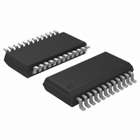
IC REMOTE THERMAL CTRLR 24-QSOP
Manufacturer
ON Semiconductor
Series
dBCool®r
Datasheet
1.ADT7463ARQZ-REEL.pdf
(52 pages)
Specifications of ADT7463ARQZ
Function
Fan Control, Temp Monitor
Topology
ADC, Comparator, Fan Speed Counter, Multiplexer, Register Bank
Sensor Type
External & Internal
Sensing Temperature
-40°C ~ 120°C, External Sensor
Output Type
SMBus™
Output Alarm
No
Output Fan
Yes
Voltage - Supply
3 V ~ 5.5 V
Operating Temperature
-40°C ~ 120°C
Mounting Type
Surface Mount
Package / Case
24-QSOP
Lead Free Status / RoHS Status
Lead free / RoHS Compliant
Available stocks
Company
Part Number
Manufacturer
Quantity
Price

Part Number:
ADT7463ARQZ
Manufacturer:
ADI/亚德诺
Quantity:
20 000
Company:
Part Number:
ADT7463ARQZ-REEL
Manufacturer:
ONSEMI
Quantity:
2 785
Part Number:
ADT7463ARQZ-REEL
Manufacturer:
ON/安森美
Quantity:
20 000


VID CODE MONITORING
The ADT7463 has five dedicated voltage ID (VID code) inputs.
These are digital inputs that can be read back through the
VID register (Reg. 0x43) to determine the processor voltage
required/being used in the system. Five VID code inputs support
VRM9.x solutions. In addition, Pin 21 (12 V input) can be recon-
figured as a sixth VID input to satisfy future VRM requirements.
VID CODE REGISTER – Register 0x43
<0> = VID0 (reflects logic state of Pin 5)
<1> = VID1 (reflects logic state of Pin 6)
<2> = VID2 (reflects logic state of Pin 7)
<3> = VID3 (reflects logic state of Pin 8)
<4> = VID4 (reflects logic state of Pin 19)
<5> = VID5 (reconfigurable 12 V input). This bit reads 0 when
Pin 21 is configured as the 12 V input. This bit reflects the logic
state of Pin 21 when the pin is configured as VID5.
VID CODE INPUT THRESHOLD VOLTAGE
The switching threshold for the VID code inputs is approximately
1 V. To enable future compatibility, it is possible to reduce the
VID code input threshold to 0.6 V. Bit 6 (THLD) of VID register
(Reg. 0x43) controls the VID input threshold voltage.
VID CODE REGISTER – Register 0x43
<6> THLD = 0; VID Switching Threshold = 1 V,
RECONFIGURING PIN 21 (+12V/VID5) AS VID5 INPUT
Pin 21 can be reconfigured as a sixth VID code input (VID5)
for VRM10-compatible systems. Since the pin is configured as
VID5, it is no longer possible to monitor a 12 V supply.
Bit 7 of the VID register (Reg. 0x43) determines the function of
Pin 21. System or BIOS software can read the state of Bit 7 to
determine whether the system is designed to monitor 12 V or is
monitoring a sixth VID input.
VID CODE REGISTER – Register 0x43
<7> VIDSEL = 0; Pin 21 functions as a 12 V measurement
input. Software can read this bit to determine that there are five
VID inputs being monitored. Bit 5 of Register 0x43 (VID5)
always reads back 0. Bit 0 of Status Register 2 (Reg. 0x42)
reflects 12 V out-of-limit measurements.
VIDSEL = 1; Pin 21 functions as the sixth VID code input
(VID5). Software can read this bit to determine that there are
six VID inputs being monitored. Bit 5 of Register 0x43 reflects
the logic state of Pin 21. Bit 0 of Status Register 2 (Reg. 0x42)
reflects VID code changes.
VID CODE CHANGE DETECT FUNCTION
The ADT7463 has a VID code change detect function. When
Pin 21 is configured as the VID5 input, VID code changes can
be detected and reported back by the ADT7463. Bit 0 of Status
Register 2 (Reg. 0x42) is the 12V/VC bit and denotes a VID
change when set. The VID code change bit gets set when the
REV. C
V
THLD = 1; VID Switching Threshold = 0.6 V,
V
OL
OL
< 0.8 V, V
< 0.4 V, V
IH
IH
> 1.7 V, V
> 0.8 V, V
MAX
MAX
= 3.3 V
= 3.3 V
Rev. 4 | Page 15 of 52 | www.onsemi.com
–15–
logic states on the VID inputs are different than they were 11 µs
previously. The change of VID code can be used to generate
an SMBALERT interrupt. If an SMBALERT interrupt is
not required, Bit 0 of Interrupt Mask Register 2 (Reg. 0x75),
when set, prevents SMBALERTs from occurring on VID code
changes.
STATUS REGISTER 2 – Register 0x42
<0> 12V/VC = 0; If Pin 21 is configured as VID5, then a
Logic 0 denotes no change in VID code within last 11 µs.
<0> 12V/VC = 1; If Pin 21 is configured as VID5, then a Logic 1
means that a change has occurred on the VID code inputs within
the last 11 µs. An SMBALERT generates if this function is en-
abled.
ADDITIONAL ADC FUNCTIONS
A number of other functions are available on the ADT7463 to
offer the systems designer increased flexibility, including:
Turn-Off Averaging
For each voltage measurement read from a value register,
16 readings have actually been made internally and the results
averaged before being placed into the value register. There may
be an instance where you would like to speed up conversions.
Setting Bit 4 of Configuration Register 2 (Reg. 0x73) turns
averaging off. This effectively gives a reading 16 times faster
(711 µs), but the reading may be noisier.
Bypass Voltage Input Attenuators
Setting Bit 5 of Configuration Register 2 (Reg 0x73) removes
the attenuation circuitry from the 2.5 V, V
12 V inputs. This allows the user to directly connect external
sensors or rescale the analog voltage measurement inputs for
other applications. The input range of the ADC without the
attenuators is 0 V to 2.25 V.
Single-Channel ADC Conversion
Setting Bit 6 of Configuration Register 2 (Reg. 0x73) places the
ADT7463 into single-channel ADC conversion mode. In this mode,
the ADT7463 can be made to read a single voltage channel
only. If the internal ADT7463 clock is used, the selected input
is read every 711 µs. The appropriate ADC channel is selected
by writing to Bits <7:5> of the TACH1 Minimum High Byte
Register (0x55).
Bits <7:5>
Reg 0x55
000
001
010
011
100
Configuration Register 2 (Reg. 0x73)
<4> = 1 Averaging Off
<5> = 1 Bypass Input Attenuators
<6> = 1 Single-Channel Convert Mode
TACH1 Minimum High Byte (Reg. 0x55)
<7:5> Selects ADC Channel for Single-Channel Convert Mode
Channel
Selected
2.5 V
V
V
5 V
12 V
CCP
CC
CCP
ADT7463
, V
CC
, 5 V, and
Related parts for ADT7463ARQZ
Image
Part Number
Description
Manufacturer
Datasheet
Request
R

Part Number:
Description:
ON Semiconductor [VOLTAGE REGULATOR]
Manufacturer:
ON Semiconductor
Datasheet:
Part Number:
Description:
357-036-542-201 CARDEDGE 36POS DL .156 BLK LOPRO
Manufacturer:
ON Semiconductor
Datasheet:
Part Number:
Description:
357-036-542-201 CARDEDGE 36POS DL .156 BLK LOPRO
Manufacturer:
ON Semiconductor
Datasheet:
Part Number:
Description:
357-036-542-201 CARDEDGE 36POS DL .156 BLK LOPRO
Manufacturer:
ON Semiconductor
Datasheet:
Part Number:
Description:
357-036-542-201 CARDEDGE 36POS DL .156 BLK LOPRO
Manufacturer:
ON Semiconductor
Datasheet:
Part Number:
Description:
357-036-542-201 CARDEDGE 36POS DL .156 BLK LOPRO
Manufacturer:
ON Semiconductor
Datasheet:
Part Number:
Description:
357-036-542-201 CARDEDGE 36POS DL .156 BLK LOPRO
Manufacturer:
ON Semiconductor
Datasheet:
Part Number:
Description:
357-036-542-201 CARDEDGE 36POS DL .156 BLK LOPRO
Manufacturer:
ON Semiconductor
Datasheet:
Part Number:
Description:
357-036-542-201 CARDEDGE 36POS DL .156 BLK LOPRO
Manufacturer:
ON Semiconductor
Datasheet:
Part Number:
Description:
357-036-542-201 CARDEDGE 36POS DL .156 BLK LOPRO
Manufacturer:
ON Semiconductor
Datasheet:
Part Number:
Description:
357-036-542-201 CARDEDGE 36POS DL .156 BLK LOPRO
Manufacturer:
ON Semiconductor
Datasheet:
Part Number:
Description:
Manufacturer:
ON Semiconductor
Datasheet:
Part Number:
Description:
Manufacturer:
ON Semiconductor
Datasheet:
Part Number:
Description:
Manufacturer:
ON Semiconductor
Datasheet: