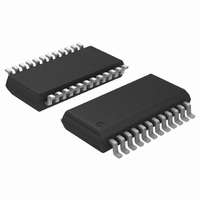
ADT7463ARQZ ON Semiconductor, ADT7463ARQZ Datasheet - Page 12

ADT7463ARQZ
Manufacturer Part Number
ADT7463ARQZ
Description
IC REMOTE THERMAL CTRLR 24-QSOP
Manufacturer
ON Semiconductor
Series
dBCool®r
Datasheet
1.ADT7463ARQZ-REEL.pdf
(52 pages)
Specifications of ADT7463ARQZ
Function
Fan Control, Temp Monitor
Topology
ADC, Comparator, Fan Speed Counter, Multiplexer, Register Bank
Sensor Type
External & Internal
Sensing Temperature
-40°C ~ 120°C, External Sensor
Output Type
SMBus™
Output Alarm
No
Output Fan
Yes
Voltage - Supply
3 V ~ 5.5 V
Operating Temperature
-40°C ~ 120°C
Mounting Type
Surface Mount
Package / Case
24-QSOP
Lead Free Status / RoHS Status
Lead free / RoHS Compliant
Available stocks
Company
Part Number
Manufacturer
Quantity
Price
Part Number:
ADT7463ARQZ
Manufacturer:
ADI/亚德诺
Quantity:
20 000
Company:
Part Number:
ADT7463ARQZ-REEL
Manufacturer:
ONSEMI
Quantity:
2 785
Part Number:
ADT7463ARQZ-REEL
Manufacturer:
ON/安森美
Quantity:
20 000
ADT7463
ADT7463 WRITE OPERATIONS
The SMBus specification defines several protocols for different
types of read and write operations. The ones used in the ADT7463
are discussed below. The following abbreviations are used in the
diagrams:
S – START
P – STOP
R – READ
W – WRITE
A – ACKNOWLEDGE
A – NO ACKNOWLEDGE
The ADT7463 uses the following SMBus write protocols.
Send Byte
In this operation, the master device sends a single command
byte to a slave device as follows:
1. The master device asserts a start condition on SDA.
2. The master sends the 7-bit slave address followed by the
3. The addressed slave device asserts ACK on SDA.
4. The master sends a command code.
5. The slave asserts ACK on SDA.
6. The master asserts a stop condition on SDA and the
For the ADT7463, the send byte protocol is used to write a
register address to RAM for a subsequent single byte read from
the same address. This is illustrated in Figure 10.
If it is required to read data from the register immediately after
setting up the address, the master can assert a repeat start con-
dition immediately after the final ACK and carry out a single
byte read without asserting an intermediate stop condition.
Write Byte
In this operation, the master device sends a command byte and
one data byte to the slave device as follows:
1. The master device asserts a start condition on SDA.
2. The master sends the 7-bit slave address followed by the
3. The addressed slave device asserts ACK on SDA.
4. The master sends a command code.
5. The slave asserts ACK on SDA.
6. The master sends a data byte.
7. The slave asserts ACK on SDA.
8. The master asserts a stop condition on SDA to end the
This is illustrated in Figure 11.
Figure 10. Setting a Register Address for Subsequent Read
write bit (low).
write bit (low).
transaction.
transaction ends.
Figure 11. Single Byte Write to a Registe r
1
S
ADDRESS
SLAVE
1
S
2
ADDRESS
SLAVE
2
W A
3
W A
REGISTER
ADDRESS
3
4
REGISTER
ADDRESS
4
5
A DATA A P
5
A P
6
6
7 8
Rev. 4 | Page 12 of 52 | www.onsemi.com
–12–
ADT7463 READ OPERATIONS
The ADT7463 uses the following SMBus read protocols.
Receive Byte
This is useful when repeatedly reading a single register. The
register address needs to have been set up previously. In this
operation, the master device receives a single byte from a slave
device as follows:
1. The master device asserts a start condition on SDA.
2. The master sends the 7-bit slave address followed by the
3. The addressed slave device asserts ACK on SDA.
4. The master receives a data byte.
5. The master asserts NO ACK on SDA.
6. The master asserts a stop condition on SDA and the trans-
In the ADT7463, the receive byte protocol is used to read a
single byte of data from a register whose address has previously
been set by a send byte or write byte operation.
ALERT RESPONSE ADDRESS
Alert response address (ARA) is a feature of SMBus devices that
allows an interrupting device to identify itself to the host when
multiple devices exist on the same bus.
The SMBALERT output can be used as an interrupt output or
can be used as an SMBALERT. One or more outputs can be
connected to a common SMBALERT line connected to the
master. If a device’s SMBALERT line goes low, the following
procedure occurs:
1. SMBALERT is pulled low.
2. Master initiates a read operation and sends the alert response
3. The device whose SMBALERT output is low responds to
4. If more than one device’s SMBALERT output is low, the one
5. Once the ADT7463 has responded to the alert response
SMBUS TIMEOUT
The ADT7463 includes an SMBus timeout feature. If there is
no SMBus activity for 35 ms, the ADT7463 assumes that the bus
is locked and releases the bus. This prevents the device from
locking or holding the SMBus expecting data. Some SMBus
controllers cannot handle the SMBus timeout feature, so it
can be disabled.
CONFIGURATION REGISTER 1 – Register 0x40
<6> TODIS = 0; SMBus Timeout ENABLED (Default)
<6> TODIS = 1; SMBus Timeout DISABLED
read bit (high).
action ends.
address (ARA = 0001 100). This is a general call address
that must not be used as a specific device address.
the alert response address, and the master reads its device
address. The address of the device is now known and it can
be interrogated in the usual way.
with the lowest device address will have priority in accordance
with normal SMBus arbitration.
address, the master must read the status registers and the
SMBALERT will only be cleared if the error condition has
gone away.
Figure 12. Single Byte Read from a Register
1
S
ADDRESS
SLAVE
2
R A DATA A P
3
4
5
6
REV. C


