ADT7473ARQZ-1R7 ON Semiconductor, ADT7473ARQZ-1R7 Datasheet - Page 60
ADT7473ARQZ-1R7
Manufacturer Part Number
ADT7473ARQZ-1R7
Description
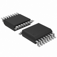
IC THERM MON FAN CTLR 16-QSOP
Manufacturer
ON Semiconductor
Series
dBCool®r
Datasheet
1.ADT7473ARQZ-1RL.pdf
(74 pages)
Specifications of ADT7473ARQZ-1R7
Function
Fan Control, Temp Monitor
Topology
ADC, Comparator, Fan Speed Counter, Multiplexer, Register Bank
Sensor Type
External & Internal
Sensing Temperature
-40°C ~ 125°C, External Sensor
Output Type
SMBus™
Output Alarm
No
Output Fan
Yes
Voltage - Supply
3 V ~ 3.6 V
Operating Temperature
-40°C ~ 125°C
Mounting Type
Surface Mount
Package / Case
16-QSOP
Full Temp Accuracy
+/- 0.5 C
Digital Output - Bus Interface
Serial (3-Wire, 4-Wire)
Maximum Operating Temperature
+ 125 C
Minimum Operating Temperature
- 40 C
Lead Free Status / RoHS Status
Lead free / RoHS Compliant
Available stocks
Company
Part Number
Manufacturer
Quantity
Price
Company:

Part Number:
ADT7473ARQZ-1R7
Manufacturer:
ON Semiconductor
Quantity:
500
Part Number:
ADT7473ARQZ-1R7
Manufacturer:
ADI/亚德诺
Quantity:
20 000


Table 24. Maximum PWM Duty Cycle Registers (Power−On Default = 0xFF)
1. These registers set the maximum PWM duty cycle of the PWM output.
2. These registers become read−only when the Configuration Register 1 lock bit is set to 1. Any subsequent attempts to write to this register fail.
3. If Bit 3 of Configuration Register 4 (0x7D) is set, then on a THERM overtemperature event, fans go to their maximum programmed PWM value
Table 25. Register 0x40 — Configuration Register 1 (Power−On Default = 0x01)
Table 26. Register 0x41 — Interrupt Status Register 1 (Power−On Default = 0x00)
Bit No.
Bit No.
Register Address
[0]
[1]
[2]
[3]
[4]
[5]
[6]
[7]
[1]
[2]
[4]
[5]
[6]
[7]
as programmed here. If Bit 3 of Configuration Register 4 (0x7D) is 0, then on a THERM overtemperature event, fans go to 100% PWM.
0x3A
0x38
0x39
Latch Reset
Mnemonic
Mnemonic
FSPDIS
TODIS
LOCK
STRT
FSPD
V
RDY
OOL
RES
V
R1T
R2T
Vx1
LT
CCP
CC
R/W (Note 2)
Write once
Read−only
Read−only
Read−only
Read−only
Read−only
Read−only
Read−only
R/W
R/W
R/W
R/W
R/W
R/W
R/W
R/W
R/W
R/W
Logic 1 enables monitoring and PWM control outputs based on the limit settings
programmed. Logic 0 disables monitoring and PWM control based on the default powerup
limit settings. This bit is not locked when Bit 1 (LOCK bit) has been written. This bit remains
writable after lock bit is set.
Logic 1 locks all limit values to their current settings. Once this bit is set, all lockable registers
become read−only and cannot be modified until the ADT7473/ADT7473−1 is powered down
and powered up again. This prevents rogue programs, such as viruses, from modifying
critical system limit settings. (This is a lockable bit.)
This bit is set to 1 by the ADT7473/ADT7473−1 to indicate only that the device is fully
powered up and ready to begin system monitoring.
When set to 1, this bit runs all fans at maximum speed as programmed in the maximum
PWM duty cycle registers (0x30, 0x38, 0x39 and 0x3A ). Power−on default = 0. This bit is not
locked at any time.
BIOS should set this bit to a 1 when the ADT7473/ADT7473−1 is configured to measure
current from an ADI ADOPT VRM controller and to measure the CPU’s core voltage. This
bit allows monitoring software to display CPU watts usage. (This is a lockable bit.)
Logic 1 disables fan spin−up for two TACH pulses. Instead, the PWM outputs go high for the
entire fan spin−up timeout selected.
When this bit is set to 1, the SMBus timeout feature is enabled. This allows the
ADT7473/ADT7473−1 to be used with SMBus controllers that cannot handle SMBus
timeouts. (This is a lockable bit.)
Reserved on the ADT7473.
On the ADT7473−1, resets latch conditions when set to 1.
V
read of the status register only if the error condition has subsided.
V
of the status register only if the error condition has subsided.
R1T = 1 indicates the Remote 1 low or high temperature has been exceeded. This bit is
cleared on a read of the status register only if the error condition has subsided.
LT = 1 indicates the local low or high temperature has been exceeded. This bit is cleared on
a read of the status register only if the error condition has subsided.
R2T = 1 indicates the Remote 2 low or high temperature has been exceeded. This bit is
cleared on a read of the status register only if the error condition has subsided.
OOL = 1 indicates an out−of−limit event has been latched in Interrupt Status Register 2
(0x42). This bit is a logical OR of all status bits in Interrupt Status Register 2. Software can
test this bit in isolation to determine whether any of the voltage, temperature, or fan speed
readings represented by Interrupt Status Register 2 are out−of−limit, which saves the need to
read Interrupt Status Register 2 every interrupt or polling cycle.
CCP
CC
Maximum duty cycle for PWM1 output, default = 100% (0xFF).
Maximum duty cycle for PWM2 output, default = 100% (0xFF).
Maximum duty cycle for PWM3 output, default = 100% (0xFF).
= 1 indicates the V
= 1 indicates the V
http://onsemi.com
CC
60
CCP
high or low limit has been exceeded. This bit is cleared on a read
high or low limit has been exceeded. This bit is cleared on a
Description
Description
Description
(Note 1, 2, and 3)
Related parts for ADT7473ARQZ-1R7
Image
Part Number
Description
Manufacturer
Datasheet
Request
R

Part Number:
Description:
ON Semiconductor [VOLTAGE REGULATOR]
Manufacturer:
ON Semiconductor
Datasheet:
Part Number:
Description:
357-036-542-201 CARDEDGE 36POS DL .156 BLK LOPRO
Manufacturer:
ON Semiconductor
Datasheet:
Part Number:
Description:
357-036-542-201 CARDEDGE 36POS DL .156 BLK LOPRO
Manufacturer:
ON Semiconductor
Datasheet:
Part Number:
Description:
357-036-542-201 CARDEDGE 36POS DL .156 BLK LOPRO
Manufacturer:
ON Semiconductor
Datasheet:
Part Number:
Description:
357-036-542-201 CARDEDGE 36POS DL .156 BLK LOPRO
Manufacturer:
ON Semiconductor
Datasheet:
Part Number:
Description:
357-036-542-201 CARDEDGE 36POS DL .156 BLK LOPRO
Manufacturer:
ON Semiconductor
Datasheet:
Part Number:
Description:
357-036-542-201 CARDEDGE 36POS DL .156 BLK LOPRO
Manufacturer:
ON Semiconductor
Datasheet:
Part Number:
Description:
357-036-542-201 CARDEDGE 36POS DL .156 BLK LOPRO
Manufacturer:
ON Semiconductor
Datasheet:
Part Number:
Description:
357-036-542-201 CARDEDGE 36POS DL .156 BLK LOPRO
Manufacturer:
ON Semiconductor
Datasheet:
Part Number:
Description:
357-036-542-201 CARDEDGE 36POS DL .156 BLK LOPRO
Manufacturer:
ON Semiconductor
Datasheet:
Part Number:
Description:
357-036-542-201 CARDEDGE 36POS DL .156 BLK LOPRO
Manufacturer:
ON Semiconductor
Datasheet:
Part Number:
Description:
Manufacturer:
ON Semiconductor
Datasheet:
Part Number:
Description:
Manufacturer:
ON Semiconductor
Datasheet:
Part Number:
Description:
Manufacturer:
ON Semiconductor
Datasheet: