ISL62392HRTZ Intersil, ISL62392HRTZ Datasheet - Page 19
ISL62392HRTZ
Manufacturer Part Number
ISL62392HRTZ
Description
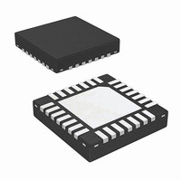
IC PWR SUPPLY CONTROLLER 28TQFN
Manufacturer
Intersil
Datasheet
1.ISL62391HRTZ.pdf
(20 pages)
Specifications of ISL62392HRTZ
Applications
Power Supply Controller
Voltage - Supply
5.5 V ~ 25 V
Current - Supply
150µA
Operating Temperature
-10°C ~ 100°C
Mounting Type
Surface Mount
Package / Case
28-TQFN
Lead Free Status / RoHS Status
Lead free / RoHS Compliant
Voltage - Input
-
Available stocks
Company
Part Number
Manufacturer
Quantity
Price
Company:

Part Number:
ISL62392HRTZ
Manufacturer:
Intersil
Quantity:
35
Part Number:
ISL62392HRTZ
Manufacturer:
INTESIL
Quantity:
20 000
Part Number:
ISL62392HRTZ-T
Manufacturer:
INTERSIL
Quantity:
20 000


R
connect C
ISEN resistor should also be connected to the output pad of
the inductor with a separate trace. Connect the OCSET pin
to the common node of node of R
For resistive current sensing, connect R
OCSET pin to the inductor side of the resistor pad. The ISEN
resistor should be connected to the V
pad.
In both current-sense configurations, the resistor and
capacitor sensing elements, with the exclusion of the current
sense power resistor, should be placed near the
corresponding IC pin. The trace connections to the inductor
or sensing resistor should be treated as Kelvin connections.
FB (Pins 7 and 28), and VOUT (Pins 8 and 27)
The VOUT pin is used to generate the R
voltage and for soft-discharge of the output voltage during
shutdown events. This signal should be routed as close to
the regulation point as possible. The input impedance of the
FB pin is high, so place the voltage programming and loop
compensation components close to the VOUT, FB, and GND
pins, keeping the high impedance trace short.
FSET (Pins 2 and 6)
This pin requires a quiet environment. The resistor R
and capacitor C
this pin. Keep fast moving nodes away from this pin.
LGATE (Pins 15 and 20)
The signal going through this trace is both high dv/dt and
high di/dt, with high peak charging and discharging current.
Route this trace in parallel with the trace from the PGND pin.
These two traces should be short, wide, and away from
other traces. There should be no other weak signal traces in
proximity with these traces on any layer.
Intersil products are sold by description only. Intersil Corporation reserves the right to make changes in circuit design, software and/or specifications at any time without
notice. Accordingly, the reader is cautioned to verify that data sheets are current before placing orders. Information furnished by Intersil is believed to be accurate and
reliable. However, no responsibility is assumed by Intersil or its subsidiaries for its use; nor for any infringements of patents or other rights of third parties which may result
from its use. No license is granted by implication or otherwise under any patent or patent rights of Intersil or its subsidiaries.
OCSET
to the phase-node side pad of the inductor, and
SEN
All Intersil U.S. products are manufactured, assembled and tested utilizing ISO9000 quality systems.
to the output side pad of the inductor. The
FSET
Intersil Corporation’s quality certifications can be viewed at www.intersil.com/design/quality
should be placed directly adjacent to
For information regarding Intersil Corporation and its products, see www.intersil.com
19
OCSET
ISL62391, ISL62392, ISL62391C, ISL62392C
OUT
OCSET
3
and C
side of the resistor
synthetic ramp
SEN
from the
.
FSET
BOOT (Pins 14 and 21), UGATE (Pins 13 and 22), and
PHASE (Pins 12 and 23)
The signals going through these traces are both high dv/dt
and high di/dt, with high peak charging and discharging
current. Route the UGATE and PHASE pins in parallel with
short and wide traces. There should be no other weak signal
traces in proximity with these traces on any layer.
Copper Size for the Phase Node
The parasitic capacitance and parasitic inductance of the
phase node should be kept very low to minimize ringing. It is
best to limit the size of the PHASE node copper in strict
accordance with the current and thermal management of the
application. An MLCC should be connected directly across
the drain of the upper MOSFET and the source of the lower
MOSFET to suppress the turn-off voltage spike.
April 7, 2011
FN6666.5
Related parts for ISL62392HRTZ
Image
Part Number
Description
Manufacturer
Datasheet
Request
R

Part Number:
Description:
Intersil Corporation [CMOS Serial Controller Interface]
Manufacturer:
Intersil Corporation
Datasheet:
Part Number:
Description:
Manufacturer:
Intersil Corporation
Datasheet:
Part Number:
Description:
357-036-542-201 CARDEDGE 36POS DL .156 BLK LOPRO
Manufacturer:
Intersil Corporation
Datasheet:
Part Number:
Description:
1024-Word x 4-Bit LSI Static RAM
Manufacturer:
Intersil Corporation
Datasheet:
Part Number:
Description:
General Purpose NPN Transistor Arrays FN341.4
Manufacturer:
Intersil Corporation
Datasheet:
Part Number:
Description:
CMOS 16-Bit Microprocessor
Manufacturer:
Intersil Corporation
Datasheet:
Part Number:
Description:
Manufacturer:
Intersil Corporation
Datasheet:
Part Number:
Description:
Manufacturer:
Intersil Corporation
Datasheet:
Part Number:
Description:
Manufacturer:
Intersil Corporation
Datasheet:
Part Number:
Description:
Manufacturer:
Intersil Corporation
Datasheet:
Part Number:
Description:
CMOS 6-Bit Latch and Decoder Memory Interfaces
Manufacturer:
Intersil Corporation
Datasheet:
Part Number:
Description:
CA3046General Purpose NPN Transistor Arrays
Manufacturer:
Intersil Corporation
Datasheet:
Part Number:
Description:
Manufacturer:
Intersil Corporation
Datasheet:
Part Number:
Description:
TR909 DLC/FLC SLIC with Low Power Standby
Manufacturer:
Intersil Corporation
Datasheet:
Part Number:
Description:
Manufacturer:
Intersil Corporation
Datasheet: