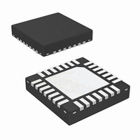
ISL62392HRTZ Intersil, ISL62392HRTZ Datasheet - Page 16

ISL62392HRTZ
Manufacturer Part Number
ISL62392HRTZ
Description
IC PWR SUPPLY CONTROLLER 28TQFN
Manufacturer
Intersil
Datasheet
1.ISL62391HRTZ.pdf
(20 pages)
Specifications of ISL62392HRTZ
Applications
Power Supply Controller
Voltage - Supply
5.5 V ~ 25 V
Current - Supply
150µA
Operating Temperature
-10°C ~ 100°C
Mounting Type
Surface Mount
Package / Case
28-TQFN
Lead Free Status / RoHS Status
Lead free / RoHS Compliant
Voltage - Input
-
Available stocks
Company
Part Number
Manufacturer
Quantity
Price
Company:
Part Number:
ISL62392HRTZ
Manufacturer:
Intersil
Quantity:
35
Part Number:
ISL62392HRTZ
Manufacturer:
INTESIL
Quantity:
20 000
Part Number:
ISL62392HRTZ-T
Manufacturer:
INTERSIL
Quantity:
20 000
Compensation Design
Figure 27 shows the recommended Type-II compensation
circuit. The FB pin is the inverting input of the error amplifier.
The COMP signal, the output of the error amplifier, is inside the
chip and unavailable to users. C
integrated inside the IC that connects across the FB pin and the
COMP signal. R
compensator. The frequency domain transfer function is given
by Equation 15:
The LC output filter has a double pole at its resonant frequency
that causes rapid phase change. The R
ISL62391, ISL62392, ISL62391C and ISL62392C make the LC
output filter resemble a first order system in which the closed
loop stability can be achieved with the recommended Type-II
compensation network. Intersil provides a PC-based tool
(example page is shown later) that can be used to calculate
compensation network component values and help simulate
the loop frequency response.
3.3V Linear Regulator
In addition to the two SMPS outputs, the ISL62391, ISL62392,
ISL62391C and ISL62392C also provide a fixed 3.3V LDO
output (LDO3) capable of sourcing 100mA continuous current.
LDO3 draws its power from PVCC and can be independently
enabled from both SMPS channels.
LDO3 also has a current limit feature with a nominal level of
180mA. Currents in excess of the limit will cause the LDO3
voltage to drop dramatically, limiting the power dissipation.
Thermal Monitor and Protection
LDO3 and PVCC LDOs can dissipate non-trivial power inside
the ISL62391, ISL62392, ISL62391C and ISL62392C at high
input-to-output voltage ratios and full load conditions. To protect
the silicon, ISL62391, ISL62392, ISL62391C and ISL62392C
continually monitor the die temperature. If the temperature
G
R
BOTTOM
COMP
COMP
ISL62391, ISL62392
FIGURE 27. COMPENSATION REFERENCE CIRCUIT
C
s ( )
INT
=
=
= 100pF
REF
EA
------------------------------------ -
V
-------------------------------------------------------------------------------------------
s R
V
OUT
•
REF
TOP
+
-
1
TOP
+
•
–
, R
FB
R
s R
V
•
TOP
•
FB
REF
C
(
INT
, C
TOP
FB
•
(
R
16
1
+
BOTTOM
R
and C
+
INT
R
FB
s R
FB
•
ISL62391, ISL62392, ISL62391C, ISL62392C
R
is a 100pF capacitor
) C
TOP
•
FB
INT
3
FB
•
modulator used in the
C
C
form the Type-II
FB
FB
)
(EQ. 15)
(EQ. 14)
VO
exceeds +150
power dissipation. The outputs will remain off until the junction
temperature has fallen below +135
General Application Design Guide
This design guide is intended to provide a high-level
explanation of the steps necessary to design a single-phase
power converter. It is assumed that the reader is familiar with
many of the basic skills and techniques referenced in the
following section. In addition to this guide, Intersil provides
complete reference designs that include schematics, bills of
materials, and example board layouts.
Selecting the LC Output Filter
The duty cycle of an ideal buck converter is a function of the
input and the output voltage. This relationship is written as
Equation 16:
The output inductor peak-to-peak ripple current is written as
Equation 17:
I
A typical step-down DC/DC converter will have an I
20% to 40% of the maximum DC output load current. The
value of I
MOSFET switching loss, inductor core loss, and the resistive
loss of the inductor winding. The DC copper loss of the
inductor can be estimated by Equation 18:
Where I
The copper loss can be significant so attention has to be
given to the DCR selection. Another factor to consider when
choosing the inductor is its saturation characteristics at
elevated temperature. A saturated inductor could cause
destruction of circuit components, as well as nuisance OCP
faults.
A DC/DC buck regulator must have output capacitance C
into which ripple current I
corresponding ripple voltage V
sum of the voltage drop across the capacitor ESR and of the
voltage change stemming from charge moved in and out of
the capacitor. These two voltages are written as Equation 19:
and Equation 20:
If the output of the converter has to support a load with high
pulsating current, several capacitors will need to be paralleled
to reduce the total ESR until the required V
D
P
ΔV
ΔV
PP
COPPER
=
ESR
C
=
---------
V
V
=
IN
V
----------------------------- -
O
-----------------------------
8 C
O
LOAD
=
f
•
SW
P-P
•
I
(
I
=
P-P
1 D
P-P
O
•
–
is selected based upon several criteria, such as
I
•
L
°
LOAD
f
is the converter output DC current.
•
C, all outputs will be turned off to sharply curtail
SW
E
)
SR
2
•
DCR
P-P
can flow. Current I
P-P
°
across C
C.
P-P
O,
which is the
P-P
is achieved.
develops a
P-P
April 7, 2011
(EQ. 19)
(EQ. 20)
(EQ. 16)
(EQ. 18)
(EQ. 17)
FN6666.5
of
O


