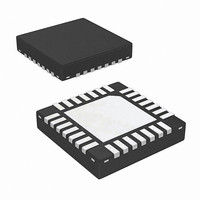
ISL62392HRTZ Intersil, ISL62392HRTZ Datasheet - Page 12

ISL62392HRTZ
Manufacturer Part Number
ISL62392HRTZ
Description
IC PWR SUPPLY CONTROLLER 28TQFN
Manufacturer
Intersil
Datasheet
1.ISL62391HRTZ.pdf
(20 pages)
Specifications of ISL62392HRTZ
Applications
Power Supply Controller
Voltage - Supply
5.5 V ~ 25 V
Current - Supply
150µA
Operating Temperature
-10°C ~ 100°C
Mounting Type
Surface Mount
Package / Case
28-TQFN
Lead Free Status / RoHS Status
Lead free / RoHS Compliant
Voltage - Input
-
Available stocks
Company
Part Number
Manufacturer
Quantity
Price
Company:
Part Number:
ISL62392HRTZ
Manufacturer:
Intersil
Quantity:
35
Part Number:
ISL62392HRTZ
Manufacturer:
INTESIL
Quantity:
20 000
Part Number:
ISL62392HRTZ-T
Manufacturer:
INTERSIL
Quantity:
20 000
Theory of Operation
Three Output Controller
The ISL62391, ISL62392, ISL62391C and ISL62392C
generate three regulated output voltages. Two are produced
with switch-mode power supplies (SMPS), and the third by a
low dropout linear regulator (LDO). An additional 5V LDO
(PVCC) is used to power the chip during operation, allowing
the ISL62391, ISL62392, ISL62391C and ISL62392C to
regulate all outputs from a single power source (VIN) with no
need for a separate quiescent supply. This makes the
ISL62391, ISL62392, ISL62391C and ISL62392C an ideal
choice as system regulator for notebook PCs. Because the
two SMPS channels are identical and almost entirely
independent, all conclusions drawn apply to both channels
unless otherwise noted.
Modulator and Switching Frequency
The ISL62391, ISL62392, ISL62391C and ISL62392C
modulator feature Intersil’s R
frequency PWM and variable frequency hysteretic control.
Intersil’s R
switching frequency and PWM duty cycle in response to
input voltage and output load transients. The R
synthesizes an AC signal, V
representation of the output inductor ripple current. The
duty-cycle of V
current through a ripple capacitor, C
C
measures the VIN and VO pin voltages. The positive slope
of V
The negative slope of V
Where g
V
V
RIPPLE CAPACITOR VOLTAGE C
RPOS
R
RNEG
FIGURE 23. MODULATOR WAVEFORMS DURING LOAD
is provided by a transconductance amplifier that
R
can be written as Equation 1:
=
=
m
g
g
3
is the gain of the transconductance amplifier.
m
m
technology can simultaneously affect the PWM
⋅
⋅
TRANSIENT
(
V
R
V
OUT
IN
is the result of charge and discharge
–
V
OUT
R
)
can be written as Equation 2:
R
12
3
R
, which is an analog
technology, a hybrid of fixed
ERROR AMPLIFIER
VOLTAGE V
ISL62391, ISL62392, ISL62391C, ISL62392C
R
WINDOW VOLTAGE V
. The current through
(WRT V
COMP
PWM
COMP
3
modulator
)
(EQ. 2)
(EQ. 1)
W
A window voltage V
amplifier output voltage V
which the ripple voltage V
V
GND pins. The V
window comparator in which V
voltage and V
shows PWM pulses being generated as V
V
is proportional to the slew rates of the positive and negative
slopes of V
between V
calculate the window size based on output voltage and
frequency set resistor.
V
The frequency can be expressed in Equation 4:
F
Inverting Equation 4 allows easy selection of R
desired F
R
For Equations 3 through 5:
Power-On Reset
The ISL62391, ISL62392, ISL62391C and ISL62392C are
disabled until the voltage at the VIN pin has increased above
the rising power-on reset (POR) threshold. Conversely, the
controller will be disabled when the voltage at the VIN pin
decreases below the falling POR threshold.
In addition to VIN POR, the PVCC pin is also monitored. If its
voltage falls below 4.2V, the SMPS outputs will be shut
down. This ensures that there is sufficient BOOT voltage to
enhance the upper MOSFET.
EN, Soft-Start and PGOOD
The ISL62391, ISL62392, ISL62391C and ISL62392C use a
digital soft-start circuit to ramp the output voltage of each
SMPS to the programmed regulation setpoint at a
predictable slew rate. The slew rate of the soft-start
sequence has been selected to limit the in-rush current
through the output capacitors as they charge to the desired
regulation voltage. When the EN pins are pulled above their
rising thresholds, the PGOOD Soft-Start Delay, t
the output voltage begins to rise. The FB pin ramps to 0.6V in
approximately 1.5ms and the PGOOD pin goes to high
impedance approximately 1.25ms after the FB pin voltage
reaches 0.6V.
SW
W
W
W
W
g
K = 1.7 x 10
D = V
is set by a resistor, R
and V
=
=
m
=
g
-------------------- -
K F
m
----------------- -
K R
= 1.66µs
⋅
⋅
⋅
SW
1
OUT
COMP
1
V
SW
W
R;
OUT
W
:
and V
W
it is inversely proportional to the voltage
/V
-10
IN
is the higher threshold voltage. Figure 23
⋅
thresholds. The PWM switching frequency
R,
(
1 D
COMP.
W
V
(±20%)
–
COMP,
is referenced with respect to the error
) R
⋅
W
COMP
R
Equation 3 illustrates how to
, connected across the FSET and
W
is compared. The amplitude of
and V
COMP
, creating an envelope into
W
signals feed into a
is the lower threshold
R
traverses the
SS
W
, starts and
for a
April 7, 2011
FN6666.5
(EQ. 3)
(EQ. 4)
(EQ. 5)


