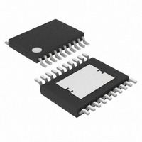
MAX16834AUP+T Maxim Integrated Products, MAX16834AUP+T Datasheet - Page 9

MAX16834AUP+T
Manufacturer Part Number
MAX16834AUP+T
Description
IC LED DRVR HIGH BRIGHT 20-TSSOP
Manufacturer
Maxim Integrated Products
Type
HBLED Driverr
Datasheet
1.MAX16834ATP.pdf
(23 pages)
Specifications of MAX16834AUP+T
Topology
PWM, SEPIC, Step-Down (Buck), Step-Up (Boost)
Number Of Outputs
1
Internal Driver
No
Type - Primary
Automotive, Backlight
Type - Secondary
High Brightness LED (HBLED), RGB
Frequency
100kHz ~ 1MHz
Voltage - Supply
4.75 V ~ 28 V
Mounting Type
Surface Mount
Package / Case
20-TSSOP Exposed Pad, 20-eTSSOP, 20-HTSSOP
Operating Temperature
-40°C ~ 125°C
Internal Switch(s)
Yes
Lead Free Status / RoHS Status
Lead free / RoHS Compliant
Voltage - Output
-
Current - Output / Channel
-
Efficiency
-
Lead Free Status / Rohs Status
Details
The MAX16834 is also suitable for DC-DC converter
applications such as boost or boost-buck (Figures 6
and 7). Other applications include boost LED drivers
with automotive load dump protection (Figure 4) and
high-side buck LED drivers (Figure 5).
The MAX16834 features an adjustable UVLO using the
enable input (UVEN). Connect UVEN to V
resistive divider to set the UVLO threshold. The
MAX16834 is enabled when the V
1.435V (typ) threshold. See the Setting the UVLO
Threshold section for more information.
UVEN also functions as an enable/disable input to the
device. Drive UVEN low to disable the output and high
to enable the output.
The MAX16834 features a 3.7V reference output, REF.
REF provides power to most of the internal circuit blocks
except for the output drivers and is capable of sourcing
1mA to external circuits. Connect a 0.1μF to 0.22μF
ceramic capacitor from REF to SGND. Connect REF to
REFI through a resistive divider to set the LED current.
The output current is proportional to the voltage at
REFI. Applying an external DC voltage at REFI or using
a potentiometer from REF to SGND allows analog dim-
ming of the output current.
LV is a reference input. Connect LV to SGND for boost
and SEPIC topologies. Connect LV to IN for boost-buck
and high-side buck topologies.
The voltage at HV provides the input voltage for the
dimming driver regulator. For boost or SEPIC topology,
connect HV either to IN or to V
nect HV to a voltage higher than IN. The voltage at HV
must not exceed 28V with respect to PGND. For the
high-side buck, connect HV to IN.
The MAX16834 requires an external n-channel MOSFET
for PWM dimming. Connect the gate of the MOSFET to
the output of the dimming driver, DIMOUT, for normal
operation. The dimming driver is capable of sinking or
sourcing up to 50mA of current.
High-Power LED Driver with Integrated High-Side LED
Current Sense and PWM Dimming MOSFET Driver
High-Side Reference Voltage Input (LV)
Dimming MOSFET Driver (DIMOUT)
Undervoltage Lockout/Enable
_______________________________________________________________________________________
Dimming Driver Regulator
Reference Voltage (REF)
Reference Input (REFI)
CC
Input Voltage (HV)
. For boost-buck, con-
UVEN
exceeds the
IN
through a
The MAX16834 drives an external n-channel switching
MOSFET. NDRV swings between V
NDRV is capable of sinking/sourcing 3A of peak current,
allowing the MAX16834 to switch MOSFETs in high-
power applications. The average current demanded
from the supply to drive the external MOSFET depends
on the total gate charge (Q
frequency of the converter, f
tion to calculate the driver supply current I
required for the switching MOSFET:
The MAX16834 offers a dimming input (PWMDIM) for
pulse-width modulating the output current. PWM dim-
ming can be achieved by driving PWMDIM with a pul-
sating voltage source. When the voltage at PWMDIM is
greater than 1.435V, the PWM dimming MOSFET turns
on and when the voltage on PWMDIM is below 1.235V,
the PWM dimming MOSFET turns off.
The MAX16834’s 5V high-side regulator (CLV) powers
up the dimming MOSFET driver. V
respect to LV and sources up to 2mA of current.
Bypass CLV to LV with a 0.1μF to 1μF low-ESR ceramic
capacitor. The maximum voltage on CLV with respect
to PGND must not exceed 28V. This limits the input volt-
age for boost-buck topology.
The MAX16834’s 7V low-side linear regulator (V
ers up the switching MOSFET driver with sourcing capa-
bility of up to 50mA. Use at least a 1μF low-ESR ceramic
capacitor from V
The differential voltage from SENSE+ to LV is fed to an
internal current-sense amplifier. This amplified signal is
then connected to the negative input of the transcon-
ductance error amplifier. The voltage gain factor of this
amplifier is 9.9 (typ).
Whenever V
of the LED current-sense amplifier seen at the SENSE+
pin is 1kΩ ±30%. In that condition, a bias current of
20μA (±30%) is pulled from SENSE+, in addition to the
current due to the 1kΩ resistor. When V
1V, the amplifier input (SENSE+ pin) is in high imped-
ance and the bias current of 20μA (±30%) is pushed
out of that pin.
Always have a bypass capacitor of at least 0.1μF value
between SENSE+ and LV and close to the IC.
n-Channel MOSFET Switch Driver (NDRV)
LED Current-Sense Input (SENSE+)
High-Side Linear Regulator (V
LV
Pulse Dimming Inputs (PWMDIM)
Low-Side Linear Regulator (V
is greater than 5V, the input impedance
CC
I
to PGND for stable operation.
NDRV
= Q
SW
G
. Use the following equa-
x f
G
) and the operating
SW
CLV
is measured with
CC
LV
and PGND.
is less than
CC
) pow-
NDRV
CLV
CC
9
)
)


