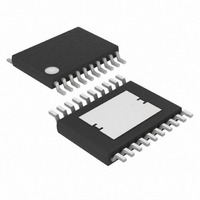
MAX16834AUP+T Maxim Integrated Products, MAX16834AUP+T Datasheet - Page 7

MAX16834AUP+T
Manufacturer Part Number
MAX16834AUP+T
Description
IC LED DRVR HIGH BRIGHT 20-TSSOP
Manufacturer
Maxim Integrated Products
Type
HBLED Driverr
Datasheet
1.MAX16834ATP.pdf
(23 pages)
Specifications of MAX16834AUP+T
Topology
PWM, SEPIC, Step-Down (Buck), Step-Up (Boost)
Number Of Outputs
1
Internal Driver
No
Type - Primary
Automotive, Backlight
Type - Secondary
High Brightness LED (HBLED), RGB
Frequency
100kHz ~ 1MHz
Voltage - Supply
4.75 V ~ 28 V
Mounting Type
Surface Mount
Package / Case
20-TSSOP Exposed Pad, 20-eTSSOP, 20-HTSSOP
Operating Temperature
-40°C ~ 125°C
Internal Switch(s)
Yes
Lead Free Status / RoHS Status
Lead free / RoHS Compliant
Voltage - Output
-
Current - Output / Channel
-
Efficiency
-
Lead Free Status / Rohs Status
Details
The MAX16834 is a current-mode, high-brightness LED
(HB LED) driver designed to control a single-string LED
current regulator with two external n-channel MOSFETs.
The MAX16834 integrates all the building blocks nec-
essary to implement a fixed-frequency HB LED driver
with wide-range dimming control. The MAX16834
allows implementation of different converter topologies
such as SEPIC, boost, boost-buck, or high-side buck
current regulator.
The MAX16834 features a constant-frequency, peak-cur-
rent-mode control with programmable slope compensa-
tion to control the duty cycle of the PWM controller. A
dimming driver offers a wide-range dimming control for
the external n-channel MOSFET in series with the LED
string. In addition to PWM dimming, the MAX16834
allows for analog dimming of LED current.
High-Power LED Driver with Integrated High-Side LED
TQFN
10
11
12
13
14
15
16
17
18
19
20
Current Sense and PWM Dimming MOSFET Driver
—
7
8
9
PIN
TSSOP
10
11
12
13
14
15
16
17
18
19
20
—
9
1
2
_______________________________________________________________________________________
RT/SYNC
PWMDIM
DIMOUT
SENSE+
NAME
PGND
NDRV
UVEN
CLV
V
FLT
CS
HV
LV
EP
IN
CC
Detailed Description
Active-Low, Open-Drain Fault Indicator Output. See the Fault Indicator ( FLT ) section.
Resistor-Programmable Switching Frequency Setting/Sync Control Input. Connect a resistor from
RT/SYNC to SGND to set the switching frequency. Drive RT/SYNC to synchronize the switching
frequency with an external clock.
Undervoltage-Lockout (UVLO) Threshold/Enable Input. UVEN is a dual-function adjustable UVLO
threshold input with an enable feature. Connect UVEN to V
program the UVLO threshold. Observe the absolute maximum value for this pin.
PWM Dimming Input. Connect to an external PWM signal for dimming operation.
Current-Sense Amplifier Positive Input. Connect a resistor from CS to PGND to set the inductor peak
current limit.
Power Ground
External n-Channel Gate-Driver Output
7V Low-Dropout Voltage Regulator. Bypass to PGND with at least a 1μF low-ESR ceramic capacitor.
V
Positive Power-Supply Input. Bypass to PGND with at least a 0.1μF ceramic capacitor.
High-Side Positive Supply Input Referred to LV. HV provides power to high-side linear regulator
5V High-Side Regulator Output. CLV provides power to the dimming MOSFET driver. Connect a
0.1μF to 1μF ceramic capacitor from CLV to LV for stable operation.
External Dimming MOSFET Gate Driver. DIMOUT is capable of sinking/sourcing 50mA.
High-Side Reference Voltage Input. Connect to SGND for boost configuration. Connect to IN for
boost-buck configuration.
LED Current-Sense Positive Input. Connect a bypass capacitor of at least 0.1μF between SENSE+
and LV close to the IC.
Exposed Pad. Connect EP to a large-area contiguous copper ground plane for effective power
dissipation. Do not use as the main IC ground connection. EP must be connected to SGND.
CC
provides power to the n-channel gate driver (NDRV).
The MAX16834 switching frequency (100kHz to 1MHz)
is adjustable using a single resistor from RT/SYNC. The
MAX16834 disables the internal oscillator and synchro-
nizes if an external clock is applied to RT/SYNC. The
switching MOSFET driver sinks and sources up to 3A,
making it suitable for high-power MOSFETs driving in
HB LED applications, and the dimming control allows
for wide PWM dimming at frequencies up to 20kHz.
The MAX16834 is suitable for boost and boost-buck
LED drivers (Figures 2 and 3).
The MAX16834 alone operates over a wide 4.75V to
28V supply range. With a voltage clamp that limits the
IN pin voltage to less than 28V, it can operate in boost
configuration for input voltages greater than 28V.
Additional features include external enable/disable
input, an on-chip oscillator, fault indicator output (FLT)
for LED open/short or overtemperature conditions, and
an overvoltage protection circuit for true differential
overvoltage protection (Figure 1).
FUNCTION
Pin Description (continued)
IN
through a resistive voltage-divider to
7


