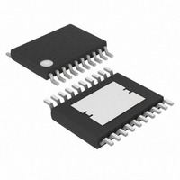
MAX16834AUP+T Maxim Integrated Products, MAX16834AUP+T Datasheet - Page 12

MAX16834AUP+T
Manufacturer Part Number
MAX16834AUP+T
Description
IC LED DRVR HIGH BRIGHT 20-TSSOP
Manufacturer
Maxim Integrated Products
Type
HBLED Driverr
Datasheet
1.MAX16834ATP.pdf
(23 pages)
Specifications of MAX16834AUP+T
Topology
PWM, SEPIC, Step-Down (Buck), Step-Up (Boost)
Number Of Outputs
1
Internal Driver
No
Type - Primary
Automotive, Backlight
Type - Secondary
High Brightness LED (HBLED), RGB
Frequency
100kHz ~ 1MHz
Voltage - Supply
4.75 V ~ 28 V
Mounting Type
Surface Mount
Package / Case
20-TSSOP Exposed Pad, 20-eTSSOP, 20-HTSSOP
Operating Temperature
-40°C ~ 125°C
Internal Switch(s)
Yes
Lead Free Status / RoHS Status
Lead free / RoHS Compliant
Voltage - Output
-
Current - Output / Channel
-
Efficiency
-
Lead Free Status / Rohs Status
Details
High-Power LED Driver with Integrated High-Side LED
Current Sense and PWM Dimming MOSFET Driver
Allowing the peak-to-peak inductor ripple (ΔI
±30% of the average inductor current:
and
The inductance value (L) of the inductor L1 in henries
(H) is calculated as:
where f
and V
Choose an inductor that has a minimum inductance
greater than the calculated value. The current rating of
the inductor should be higher than IL
temperature.
In the boost-buck LED driver (Figure 3), the average
inductor current is equal to the input current plus the
LED current.
Calculate maximum duty cycle using the following
equation:
where V
volts, V
(approximately 0.6V) in volts, V
input supply voltage in volts, and V
drain to source voltage of the MOSFET Q1 in volts when
it is on. Use an approximate value of 0.2V initially to cal-
culate D
cycle can be calculated once the power MOSFET is
selected based on the maximum inductor current.
Use the below equations to calculate the maximum
average inductor current IL
current ripple ΔI
amperes:
12
______________________________________________________________________________________
FET
D
SW
LED
MAX
are in volts, and ΔI
is the forward drop of the rectifier diode D1
D
is the switching frequency in hertz, V
MAX
. A more accurate value of maximum duty
is the forward voltage of the LED string in
L
=
L
=
ΔI
, and the peak inductor current IL
(
IL
V
V
IL
IL
L
INMIN
LED
P
AVG
=
AVG
=
Boost-Buck Configuration
IL
IL
+
AVG
f
SW
=
=
−
V
AVG
V
D
1
1
V
AVG
LED
L
FET
−
−
×
×
+
is in amperes.
I
I
LED
D
LED
D
+
Δ
0 3 2
V
, peak-to-peak inductor
.
MAX
MAX
I
)
+
INMIN
Δ
L
INMIN
×
2
I
V
×
L
D
D
FET
MAX
P
−
at the operating
is the minimum
V
is the average
FET
L
) to be
INMIN
P
in
Allowing the peak-to-peak inductor ripple ΔI
±30% of the average inductor current:
The inductance value (L) of the inductor L1 in henries is
calculated as:
where f
and V
inductor that has a minimum inductance greater than
the calculated value.
The value of the switch current-sense resistor R8 for the
boost and boost-buck configurations is calculated as
follows:
where 0.25V is the minimum peak current-sense thresh-
old, IL
the factor 1.25 provides a 25% margin to account for
tolerances. The worst cycle-by-cycle current limiter trig-
gers at 350mV (max). The I
be higher than 0.35V/R8.
The function of the output capacitor is to reduce the
output ripple to acceptable levels. The ESR, ESL, and
the bulk capacitance of the output capacitor contribute
to the output ripple. In most applications, the output
ESR and ESL effects can be dramatically reduced by
using low-ESR ceramic capacitors. To reduce the ESL
and ESR effects, connect multiple ceramic capacitors
in parallel to achieve the required bulk capacitance. To
minimize audible noise generated by the ceramic
capacitors during PWM dimming, it may be necessary
to minimize the number of ceramic capacitors on the
output. In these cases an additional electrolytic or tan-
talum capacitor provides most of the bulk capacitance.
Boost and boost-buck configurations: The calcula-
tion of the output capacitance is the same for both
boost and boost-buck configurations. The output ripple
is caused by the ESR and the bulk capacitance of the
output capacitor if the ESL effect is considered negligi-
ble. For simplicity, assume that the contributions from
FET
P
SW
is the peak inductor current in amperes, and
are in volts, and ΔI
is the switching frequency in hertz, V
Peak Current-Sense Resistor (R8)
L
=
Δ
(
V
R
IL
I
L
INMIN
8
P
=
=
=
IL
(
IL
IL
f
SW
AVG
−
P
AVG
0 25
V
.
×
L
SAT
FET
×
1 25
is in amperes. Choose an
×
Δ
. )
+
0 3 2
I
)
L
of the inductor should
.
Output Capacitor
Δ
×
2
I
Ω
D
×
L
MAX
L
to be
INMIN


