MAX16834AUP+T Maxim Integrated Products, MAX16834AUP+T Datasheet - Page 14
MAX16834AUP+T
Manufacturer Part Number
MAX16834AUP+T
Description
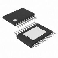
IC LED DRVR HIGH BRIGHT 20-TSSOP
Manufacturer
Maxim Integrated Products
Type
HBLED Driverr
Datasheet
1.MAX16834ATP.pdf
(23 pages)
Specifications of MAX16834AUP+T
Topology
PWM, SEPIC, Step-Down (Buck), Step-Up (Boost)
Number Of Outputs
1
Internal Driver
No
Type - Primary
Automotive, Backlight
Type - Secondary
High Brightness LED (HBLED), RGB
Frequency
100kHz ~ 1MHz
Voltage - Supply
4.75 V ~ 28 V
Mounting Type
Surface Mount
Package / Case
20-TSSOP Exposed Pad, 20-eTSSOP, 20-HTSSOP
Operating Temperature
-40°C ~ 125°C
Internal Switch(s)
Yes
Lead Free Status / RoHS Status
Lead free / RoHS Compliant
Voltage - Output
-
Current - Output / Channel
-
Efficiency
-
Lead Free Status / Rohs Status
Details


High-Power LED Driver with Integrated High-Side LED
Current Sense and PWM Dimming MOSFET Driver
configuration, the input current is the inductor current
minus the LED current. But for both configurations, the
ripple current that the input filter capacitor has to sup-
ply is the same as the inductor ripple current with the
condition that the output filter capacitor should be con-
nected to ground for boost-buck configuration. This
reduces the size of the input capacitor, as the inductor
current is continuous with maximum ±30% ripple.
Neglecting the effect of LED current ripple, the calcula-
tion of the input capacitor for boost as well as boost-
buck configurations is the same.
Neglecting the effect of the ESL, the ESR, and the bulk
capacitance at the input contributes to the input voltage
ripple. For simplicity, assume that the contribution from
the ESR and the bulk capacitance is equal. This allows
50% of the ripple for the bulk capacitance. The capaci-
tance is given by:
where ΔI
and ΔV
ripple is for the ESR of the output capacitor. Based on
this, the ESR of the input capacitor is given by:
where ΔI
is in volts.
Use the below equation to calculate the RMS current
rating of the input capacitor:
Slope compensation should be added to converters
with peak current-mode control operating in continuous
conduction mode with more than 50% duty cycle to
avoid current loop instability and subharmonic oscilla-
tions. The minimum amount of slope added to the peak
inductor current to stabilize the current control loop is
half of the falling slope of the inductor.
In the MAX16834, the slope compensating ramp is
added to the current-sense signal before it is fed to the
PWM comparator. Connect a capacitor (C2 in the appli-
cation circuit) from SC to ground for slope compensa-
tion. This capacitor is charged with a 100μA current
14
______________________________________________________________________________________
IN
L
L
is in amperes, C
is in volts. The remaining 50% of allowable
is in amperes, ESR
C
I
ESR
IN
CIN(RMS)
≥
CIN
4
×
IN
Δ
<
V
Slope Compensation
is in farads, f
=
Δ
Δ
IN
CIN
Δ
I
I
L
L
V
2
×
ΔI
IN
×
f
is in ohms, and ΔV
2
L
SW
3
SW
is in hertz,
IN
source and discharged at the beginning of each switch-
ing cycle to generate the slope compensation ramp.
The value of the slope compensation capacitor C2 is
calculated as shown below:
Boost configuration:
where C2 is in farads, L is the inductance of the induc-
tor L1 in henries, 100μA is the pullup current from SC,
V
rent-sense resistor in ohms.
Boost-buck configuration:
where C2 is in farads, L is the inductance of the induc-
tor L1 in henries, 100μA is the pullup current from SC,
V
resistor in ohms.
The switching MOSFET (Q1) should have a voltage rat-
ing sufficient to withstand the maximum output voltage
together with the diode drop of the rectifier diode D1
and any possible overshoot due to ringing caused by
parasitic inductances and capacitances. Use a
MOSFET with a drain-to-source voltage rating higher
than that calculated by the following equations:
Boost configuration:
where V
V
tor of 1.2 provides a 20% safety margin.
Boost-buck configuration:
where V
V
tor of 1.2 provides a 20% safety margin.
The continuous drain current rating of the selected
MOSFET, when the case temperature is at +70°C,
should be greater than the value calculated by the fol-
LED
LED
D
D
is the forward drop of the rectifier diode D1. The fac-
is the forward drop of the rectifier diode D1. The fac-
and V
is in volts, and R8 is the switch current-sense
DS
DS
Selection of Power Semiconductors
INMIN
V
is the drain-to-source voltage in volts and
is the drain-to-source voltage in volts and
C2
DS
C2
V
=
=
DS
are in volts, and R8 is the switch cur-
(
V
(V
=
LED
=
LED
(
3
3
V
(V
+
× ×
× ×
LED
- V
LED
L
V
L
INMAX
INMIN
+
100 10
100 10
) R8
V
×
D
×
×
)
) R8
+
× 1 2 .
×
Switching MOSFET
×
V
D
2
-
-
6
6
)
× 1 2 .
×
2
Related parts for MAX16834AUP+T
Image
Part Number
Description
Manufacturer
Datasheet
Request
R

Part Number:
Description:
High-Power LED Driver
Manufacturer:
Maxim Integrated Products
Datasheet:

Part Number:
Description:
MAX7528KCWPMaxim Integrated Products [CMOS Dual 8-Bit Buffered Multiplying DACs]
Manufacturer:
Maxim Integrated Products
Datasheet:
Part Number:
Description:
Single +5V, fully integrated, 1.25Gbps laser diode driver.
Manufacturer:
Maxim Integrated Products
Datasheet:
Part Number:
Description:
Single +5V, fully integrated, 155Mbps laser diode driver.
Manufacturer:
Maxim Integrated Products
Datasheet:
Part Number:
Description:
VRD11/VRD10, K8 Rev F 2/3/4-Phase PWM Controllers with Integrated Dual MOSFET Drivers
Manufacturer:
Maxim Integrated Products
Datasheet:
Part Number:
Description:
Highly Integrated Level 2 SMBus Battery Chargers
Manufacturer:
Maxim Integrated Products
Datasheet:
Part Number:
Description:
Current Monitor and Accumulator with Integrated Sense Resistor; ; Temperature Range: -40°C to +85°C
Manufacturer:
Maxim Integrated Products
Part Number:
Description:
TSSOP 14/A°/RS-485 Transceivers with Integrated 100O/120O Termination Resis
Manufacturer:
Maxim Integrated Products
Part Number:
Description:
TSSOP 14/A°/RS-485 Transceivers with Integrated 100O/120O Termination Resis
Manufacturer:
Maxim Integrated Products
Part Number:
Description:
QFN 16/A°/AC-DC and DC-DC Peak-Current-Mode Converters with Integrated Step
Manufacturer:
Maxim Integrated Products
Part Number:
Description:
TDFN/A/65V, 1A, 600KHZ, SYNCHRONOUS STEP-DOWN REGULATOR WITH INTEGRATED SWI
Manufacturer:
Maxim Integrated Products
Part Number:
Description:
Integrated Temperature Controller f
Manufacturer:
Maxim Integrated Products
Part Number:
Description:
SOT23-6/I°/45MHz to 650MHz, Integrated IF VCOs with Differential Output
Manufacturer:
Maxim Integrated Products
Part Number:
Description:
SOT23-6/I°/45MHz to 650MHz, Integrated IF VCOs with Differential Output
Manufacturer:
Maxim Integrated Products