LM3554TME/NOPB National Semiconductor, LM3554TME/NOPB Datasheet - Page 19
LM3554TME/NOPB
Manufacturer Part Number
LM3554TME/NOPB
Description
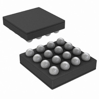
IC LED DVR PHOTO FLASH 16-USMD
Manufacturer
National Semiconductor
Type
Photo Flash LED (I²C Interface)r
Datasheet
1.LM3554TMENOPB.pdf
(40 pages)
Specifications of LM3554TME/NOPB
Constant Current
Yes
Topology
High Side, Step-Up (Boost)
Number Of Outputs
2
Internal Driver
Yes
Type - Primary
Flash/Torch
Type - Secondary
White LED
Frequency
2MHz
Voltage - Supply
2.7 V ~ 5.5 V
Voltage - Output
5V
Mounting Type
Surface Mount
Package / Case
16-MicroSMD
Operating Temperature
-30°C ~ 85°C
Current - Output / Channel
600mA
Internal Switch(s)
Yes
Efficiency
90%
Led Driver Application
LED Backlighting, Portable Electronics
No. Of Outputs
2
Output Current
1.2A
Input Voltage
2.7V To 5.5V
Dimming Control Type
I2C
Rohs Compliant
Yes
Lead Free Status / RoHS Status
Lead free / RoHS Compliant
Other names
LM3554TMETR


FLASH TERMINATION (STROBE-INITIATED FLASH)
Bit [7] of the Flash Brightness Register (STR bit) determines
how the Flash pulse terminates with STROBE-initated flash
pulses. With the STR bit = 1 the Flash current pulse will only
terminate by reaching the end of the Flash Timeout period.
With STR = 0, Flash mode can be terminated by pulling
STROBE low, or by allowing the Flash Timeout period to
elapse. If STR = 0 and STROBE is toggled before the end of
the Flash Timeout period, the Timeout period resets on the
rising edge of STROBE. See
regarding the Flash pulse termination for the different STR bit
settings.
After the Flash pulse terminates, either by a flash timeout, or
pulling STROBE low, LED1 and LED2 turn completely off.
This happens even when Torch is enabled via the I
patible interface, and the Flash pulse is turned on by toggling
STROBE. After a Flash event ends the EN1, EN0 bits (bits
[1:0] of the Torch Brightness Register, or Flash Brightness
Register) are automatically re-written with (0, 0).
FLASH TERMINATION (I
For I
terminated by either waiting for the timeout duration to expire
or by writing a (0, 0) to bits [1:0] of the Torch Brightness Reg-
ister, or Flash Brightness Register. If the timeout duration is
allowed to elapse, the flash enable bits of the Torch Bright-
ness and Flash Brightness Registers are automatically reset
to 0.
FLASH TIMEOUT
The Flash Timeout period sets the duration of the flash current
pulse. Bits [4:0] of the Flash Duration Register programs the
32 different Flash Timeout levels in steps of 32ms giving a
Flash Timeout range of 32ms to 1024ms (see
TORCH MODE
In Torch mode the current sources LED1 and LED2 each
provide 8 different current levels (see
currents are adjusted by writing to bits [5:3] of the Torch
Brightness Register. Torch mode is activated by setting Torch
Brightness Register bits [1:0] to (1, 0) or Flash Brightness bits
[1:0] to (1, 0). Once the Torch mode is enabled the current
sources will ramp up to the programmed Torch current level
by stepping through all of the Torch currents at 16µs/step until
the programmed Torch current level is reached.
TX1/TORCH
The TX1/TORCH/GPIO1 input has a triple function. With Con-
figuration Register 1 Bit [7] = 0 (default), TX1/TORCH/GPIO1
is a Power Amplifier Synchronization input (TX1 mode). This
is designed to reduce the current pulled from the battery dur-
ing an RF power amplifier transmit event. When the LM3554
is engaged in a Flash event, and the TX1 pin is pulled high,
both LED1 and LED2 are forced into Torch mode at the pro-
grammed Torch current setting. If the TX1 pin is then pulled
low before the Flash pulse terminates the LED current will
ramp back to the previous Flash current level. At the end of
the Flash timeout whether the TX1 pin is high or low, the LED
current will turn off.
With the Configuration Register Bit [7] = 1, TX1/TORCH/
GPIO1 is configured as a hardware Torch mode enable
(TORCH). In this mode a high at TORCH turns on the LED
current sources in Torch mode. STROBE (or I
will take precedence over the TORCH mode input.
12
Additionally, when a flash pulse is initiated during hardware
TORCH mode, the hardware torch mode bit is reset at the end
details the functionality of the hardware TORCH mode.
2
C initated flash pulses, the flash LED current can be
2
C-INITIATED FLASH)
LM3554 TIMING DIAGRAMS
Table
2
- initiated flash)
2). The Torch
Table
2
7).
C-com-
Figure
19
of the flash pulse. In order to re-enter hardware Torch mode,
bit [7] of Configuration Register 1 would have to be re-written
with a 1.
The TX1/TORCH/GPIO1 input can also be configured as a
GPIO input/output. for details on this, refer to the
ISTER
ENVM/TX2/GPIO2
The ENVM/TX2/GPIO2/INT pin has four functions. In ENVM
mode (Configuration Register 1 bit [5] = 0), the ENVM/TX2/
GPIO2/INT pin is an active high logic input that forces the
LM3554 into Voltage Output Mode. In TX2 mode (Configura-
tion Register 1 bit [5] = 1), the ENVM/TX2/GPIO2/INT pin is
a Power Amplifier Synchronization input that forces the
LM3554 from Flash mode into Torch mode. In GPIO2 mode
(GPIO Register Bit [3] = 1) the ENVM/TX2/GPIO2/INT pin is
configured as a general purpose logic input/output and con-
trolled via bits[3:5] of the GPIO Register. In INT mode the
ENVM/TX2/GPIO2/INT pin is a hardware interrupt output
which pulls low when the LM3554 is in NTC mode, and the
voltage at LEDI/NTC falls below V
In TX2 mode, when Configuration Register 1 bit [6] = 0 the
ENVM/TX2/GPIO2 pin is an active low transmit interrupt in-
put. Under this condition, when the LM3554 is engaged in a
Flash event, and ENVM/TX2/GPIO2 is pulled low, both LED1
and LED2 are forced into either Torch mode or LED shutdown
depending on the logic state of Configuration Register 2 bit
[0]. In TX2 mode with Configuration Register 1 bit [6] = 1, the
ENVM/TX2/GPIO2 pin is an active high transmit interrupt.
Under this condition when the LM3554 is engaged in a Flash
event, and the TX2 pin is driven high, both LED1 and LED2
are forced into Torch mode or LED shutdown, depending on
the logic state of Configuration Register 2 bit [0]. After a TX2
event, if the ENVM/TX2/GPIO2 pin is disengaged, and the
TX2 Shutdown bit is set to force Torch mode, the LED current
will ramp back to the previous Flash current level. If the TX2
shutdown bit is programmed to force LED shutdown upon a
TX2 event the Flags Register must be read to resume normal
LED operation.
tionality of the ENVM/TX2 input.
ENVM/TX2/GPIO2/INT as an Interrupt Output
In GPIO2 mode the ENVM/TX2/GPIO2 pin can be made to
reflect the inverse of the LED Thermal Fault flag (bit[5] in the
Flags Register). Configure the LM3554 for this feature by:
set GPIO Register Bit [6] = 1 (NTC External Flag)
set GPIO Register Bit [3] = 1 (GPIO2 mode)
set GPIO Register Bit [4] = 1 (GPIO2 is an output)
set Configuration Register 1 Bit [3] = 1 (NTC mode)
When the voltage at the LEDI/NTC pin falls below V
(1.05V typical), the LED Thermal Fault Flag (bit [5] in the Flags
Register) is set, and the ENVM/TX2/GPIO2/INT pin is forced
low. In this mode the interrupt can only be reset to the open-
drain state by reading back the Flags register.
INDICATOR LED/THERMISTOR (LEDI/NTC)
The LEDI/NTC pin serves a dual function, either as an LED
indicator driver or as a threshold detector for a negative tem-
perature coefficient (NTC) thermistor.
Led Indicator Mode (LEDI)
LEDI/NTC is configured as an LED indicator driver by setting
Configuration Register 1 bit [3] = (0) and Torch Brightness
Register bits [1:0] = (0, 1), or Flash Brightness Register bits
[1:0] = (0, 1). In Indicator mode there are 4 different current
levels available (2.3mA, 4.6mA, 6.9mA, 8.2mA). Bits [7:6] of
ection of the datasheet.
Table
2,
Figure 8
and
TRIP
Figure 9
.
detail the func-
www.national.com
GPIO REG-
TRIP
Related parts for LM3554TME/NOPB
Image
Part Number
Description
Manufacturer
Datasheet
Request
R

Part Number:
Description:
LM3554 PRODUCT BRIEF Synchronous Boost Converter with 1.2A Dual High Side LED Drivers and I<sup>2</sup>C Compatible Interface; Package: MICRO SMD; No of Pins: 16; Qty per Container: 250/Reel
Manufacturer:
National Semiconductor
Part Number:
Description:
National Semiconductor [8-Bit D/A Converter]
Manufacturer:
National Semiconductor
Datasheet:
Part Number:
Description:
National Semiconductor [Media Coprocessor]
Manufacturer:
National Semiconductor
Datasheet:
Part Number:
Description:
Digitally Controlled Tone and Volume Circuit with Stereo Audio Power Amplifier, Microphone Preamp Stage and National 3D Sound
Manufacturer:
National Semiconductor
Datasheet:
Part Number:
Description:
Digitally Controlled Tone and Volume Circuit with Stereo Audio Power Amplifier, Microphone Preamp Stage and National 3D Sound
Manufacturer:
National Semiconductor
Datasheet:
Part Number:
Description:
AC97 Rev 2 Codec with Sample Rate Conversion and National 3D Sound
Manufacturer:
National Semiconductor
Part Number:
Description:
Manufacturer:
National Semiconductor
Datasheet:
Part Number:
Description:
Manufacturer:
National Semiconductor
Datasheet:
Part Number:
Description:
General Purpose, Low Voltage, Low Power, Rail-to-Rail Output Operational Amplifiers
Manufacturer:
National Semiconductor
Datasheet:
Part Number:
Description:
8-bit 20 MSPS flash A/D converter.
Manufacturer:
National Semiconductor
Datasheet:
Part Number:
Description:
Low Noise Quad Operational Amplifier
Manufacturer:
National Semiconductor
Datasheet:
Part Number:
Description:
Quad Differential Line Receivers
Manufacturer:
National Semiconductor
Datasheet:
Part Number:
Description:
Quad High Speed Trapezoidal? Bus Transceiver
Manufacturer:
National Semiconductor
Datasheet:
Part Number:
Description:
Dual Line Receiver
Manufacturer:
National Semiconductor
Datasheet: