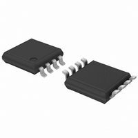
PCA9530DP,118 NXP Semiconductors, PCA9530DP,118 Datasheet - Page 7

PCA9530DP,118
Manufacturer Part Number
PCA9530DP,118
Description
IC LED DRIVER RGB 8-TSSOP
Manufacturer
NXP Semiconductors
Type
RGB LED Driverr
Datasheet
1.PCA9530D118.pdf
(24 pages)
Specifications of PCA9530DP,118
Package / Case
8-TSSOP
Topology
Open Drain, PWM
Number Of Outputs
2
Internal Driver
Yes
Type - Primary
Backlight, LED Blinker
Type - Secondary
RGB
Frequency
400kHz
Voltage - Supply
2.3 V ~ 5.5 V
Mounting Type
Surface Mount
Operating Temperature
-40°C ~ 85°C
Current - Output / Channel
25mA
Internal Switch(s)
Yes
Low Level Output Current
6.5 mA
Operating Supply Voltage
2.3 V to 5.5 V
Maximum Supply Current
500 uA
Maximum Power Dissipation
400 mW
Maximum Operating Temperature
+ 85 C
Mounting Style
SMD/SMT
Minimum Operating Temperature
- 40 C
Lead Free Status / RoHS Status
Lead free / RoHS Compliant
Voltage - Output
-
Efficiency
-
Lead Free Status / Rohs Status
Details
Other names
568-1831-2
935276297118
PCA9530DP-T
935276297118
PCA9530DP-T
Available stocks
Company
Part Number
Manufacturer
Quantity
Price
Company:
Part Number:
PCA9530DP,118
Manufacturer:
XILINX
Quantity:
1 193
NXP Semiconductors
7. Characteristics of the I
PCA9530_3
Product data sheet
7.1.1 START and STOP conditions
6.6 External RESET
7.1 Bit transfer
A reset can be accomplished by holding the RESET pin LOW for a minimum of t
PCA9530 registers and I
RESET input is once again HIGH.
This input requires a pull-up resistor to V
The I
lines are a serial data line (SDA) and a serial clock line (SCL). Both lines must be
connected to a positive supply via a pull-up resistor when connected to the output stages
of a device. Data transfer may be initiated only when the bus is not busy.
One data bit is transferred during each clock pulse. The data on the SDA line must remain
stable during the HIGH period of the clock pulse as changes in the data line at this time
will be interpreted as control signals (see
Both data and clock lines remain HIGH when the bus is not busy. A HIGH-to-LOW
transition of the data line while the clock is HIGH is defined as the START condition (S). A
LOW-to-HIGH transition of the data line while the clock is HIGH is defined as the STOP
condition (P) (see
Fig 6.
Fig 7.
2
C-bus is for 2-way, 2-line communication between different ICs or modules. The two
SDA
SCL
Bit transfer
Definition of START and STOP conditions
START condition
2
SDA
SCL
Figure
C-bus
Rev. 03 — 26 February 2009
S
2
7).
C-bus state machine will be held in their default states until the
data valid
data line
stable;
DD
Figure
if no active connection is used.
allowed
change
of data
6).
2-bit I
STOP condition
mba607
2
C-bus LED dimmer
PCA9530
P
© NXP B.V. 2009. All rights reserved.
mba608
w(rst)
. The
7 of 24


