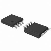
PCA9530DP,118 NXP Semiconductors, PCA9530DP,118 Datasheet - Page 6

PCA9530DP,118
Manufacturer Part Number
PCA9530DP,118
Description
IC LED DRIVER RGB 8-TSSOP
Manufacturer
NXP Semiconductors
Type
RGB LED Driverr
Datasheet
1.PCA9530D118.pdf
(24 pages)
Specifications of PCA9530DP,118
Package / Case
8-TSSOP
Topology
Open Drain, PWM
Number Of Outputs
2
Internal Driver
Yes
Type - Primary
Backlight, LED Blinker
Type - Secondary
RGB
Frequency
400kHz
Voltage - Supply
2.3 V ~ 5.5 V
Mounting Type
Surface Mount
Operating Temperature
-40°C ~ 85°C
Current - Output / Channel
25mA
Internal Switch(s)
Yes
Low Level Output Current
6.5 mA
Operating Supply Voltage
2.3 V to 5.5 V
Maximum Supply Current
500 uA
Maximum Power Dissipation
400 mW
Maximum Operating Temperature
+ 85 C
Mounting Style
SMD/SMT
Minimum Operating Temperature
- 40 C
Lead Free Status / RoHS Status
Lead free / RoHS Compliant
Voltage - Output
-
Efficiency
-
Lead Free Status / Rohs Status
Details
Other names
568-1831-2
935276297118
PCA9530DP-T
935276297118
PCA9530DP-T
Available stocks
Company
Part Number
Manufacturer
Quantity
Price
Company:
Part Number:
PCA9530DP,118
Manufacturer:
XILINX
Quantity:
1 193
NXP Semiconductors
PCA9530_3
Product data sheet
6.3.5 PWM1 - Pulse Width Modulation 1
6.3.6 LS0 - LED selector
6.4 Pins used as GPIOs
6.5 Power-on reset
The PWM1 register determines the duty cycle of BLINK1. The outputs are LOW (LED on)
when the count is less than the value in PWM1 and HIGH (LED off) when it is greater.
If PWM1 is programmed with 00h, then the PWM1 output is always HIGH (LED off).
The duty cycle of BLINK1 = PWM1 / 256.
Table 8.
The LS0 LED select register determines the source of the LED data.
Table 9.
Legend: * default value.
LEDn pins not used to control LEDs can be used as General Purpose I/Os (GPIOs).
For use as input, set LEDn to high-impedance (00) and then read the pin state via the
INPUT register.
For use as output, connect external pull-up resistor to the pin and size it according to the
DC recommended operating characteristics. LEDn output pin is HIGH when the output is
programmed as high-impedance, and LOW when the output is programmed LOW through
the ‘LED selector’ register LS0. The output can be pulse-width controlled when PWM0 or
PWM1 are used.
When power is applied to V
a reset condition until V
and the PCA9530 registers are initialized to their default states, all the outputs in the
OFF state. Thereafter, V
Bit
Symbol
Default
Register
LS0
00 = output is set high-impedance (LED off; default)
01 = output is set LOW (LED on)
10 = output blinks at PWM0 rate
11 = output blinks at PWM1 rate
PWM1 - Pulse Width Modulation 1 register description
LS0 - LED selector register bit description
PWM1
Bit
7:4
3:2
1:0
[7]
7
1
Rev. 03 — 26 February 2009
PWM1
Value
1111*
00*
00*
DD
[6]
6
0
DD
has reached V
DD
must be lowered below 0.2 V to reset the device.
, an internal Power-On Reset (POR) holds the PCA9530 in
PWM1
[5]
5
0
Description
reserved
LED1 selected
LED0 selected
POR
PWM1
[4]
4
0
. At that point, the reset condition is released
PWM1
[3]
3
0
PWM1
2-bit I
[2]
2
0
2
C-bus LED dimmer
PCA9530
© NXP B.V. 2009. All rights reserved.
PWM1
[1]
1
0
PWM1
[0]
0
0
6 of 24


