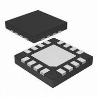
FAN5702UC30X Fairchild Semiconductor, FAN5702UC30X Datasheet - Page 14

FAN5702UC30X
Manufacturer Part Number
FAN5702UC30X
Description
IC LED DVR 6LED 30MA I2C 16WLCSP
Manufacturer
Fairchild Semiconductor
Type
Backlight, White LED (I²C Interface)r
Datasheet
1.FAN5702UC15X.pdf
(17 pages)
Specifications of FAN5702UC30X
Topology
PWM, Switched Capacitor (Charge Pump)
Number Of Outputs
6
Internal Driver
Yes
Type - Primary
Backlight
Type - Secondary
White LED
Frequency
900kHz ~ 1.5MHz
Voltage - Supply
2.7 V ~ 5.5 V
Voltage - Output
2 V ~ 4 V
Mounting Type
Surface Mount
Package / Case
16-WLCSP
Operating Temperature
-40°C ~ 85°C
Current - Output / Channel
30mA
Internal Switch(s)
Yes
Efficiency
92%
High Level Output Current
180 mA
Operating Supply Voltage
2.7 V to 5.5 V
Maximum Supply Current
4.4 mA
Maximum Operating Temperature
+ 85 C
Mounting Style
SMD/SMT
Minimum Operating Temperature
- 40 C
Lead Free Status / RoHS Status
Lead free / RoHS Compliant
Other names
FAN5702UC30XTR
© 2010 Fairchild Semiconductor Corporation
FAN5702 • Rev. 1.0.3
Register Descriptions
The following tables define the operation of each register bit. Bold values are power-up defaults. These values apply only to I
version of the part.
GENERAL
CONFIG
CHA
CH3
CH4
CH5
CH6
Bit
6,5
1,0
7:6
5:0
7:6
5:0
7:6
5:0
7:6
5:0
7:6
5:0
7
4
3
2
1
0
7
6
5
4
3
2
Brightness A
Brightness 3
Brightness 4
Brightness 5
Brightness 6
RS1, RS0
Reserved
Reserved
Reserved
Reserved
Reserved
FS1, FS2
Name
PWM
ENA
EN6
EN5
EN4
EN3
S6A
S5A
S4A
S3A
T56
T34
Default: FFH
Default: FFH
Default: FFH
Default: FFH
Default: 00H
Default: 00H
Default:
00 – 3FH
00 – 3FH
00 – 3FH
00 – 3FH
00 – 3FH
Default
Value
0 – 63
0 – 63
0 – 63
0 – 63
0 – 63
00
00
11
11
11
11
11
0
0
0
0
0
0
0
0
0
0
0
0
General Purpose Register
Configuration Register
Group A Brightness Control
Channel 3 Brightness Control
Channel 4 Brightness Control
Channel 5 Brightness Control
Channel 6 Brightness Control
Setting this bit=1 changes the EN pin to function as a PWM dimming input for
group A LEDs. This bit must be set to zero for the chip to be disabled.
00=20mA (default), 01=30mA, 10=15mA, 11=8mA when I
Default=0 (Off), LED Channel Active=1
Default=0 (Off), LED Channel Active=1
Default=0 (Off), LED Channel Active=1
Default=0 (Off), LED Channel Active=1
Default=0 (Off), LED Channel Active=1
Tie channel 5 and 6 together. Default=0 (Separate). Group 5&6 =1. Both currents
are set by CH5 register. T56 is overwritten by either S5A or S6A.
Tie channel 3 and 4 together. Default=0 (Separate). Group 3&4 =1. Both currents
are set by the CH3 register. T34 is overwritten by either S3A or S4A.
CH6 group configuration. Independent=0 (default); part of group A=1.
CH5 group configuration. Independent=0 (default); part of group A=1.
CH4 group configuration. Independent=0 (default); part of group A=1.
CH3 group configuration. Independent=0 (default); part of group A=1.
Sets current ramp rate for group A channels
Vendor ID bits. These bits can be used to distinguish between vendors via I
Writing to these bits does not change their value.
6-bit value that controls group A brightness per values in Table 1
Writing to these bits does not change their value.
6-bit value that controls channel 3 brightness per values in Table 1
Writing to these bits does not change their value.
6-bit value that controls channel 3 brightness per values in Table 1
Writing to these bits does not change their value.
6-bit value that controls channel 3 brightness per values in Table 1
Writing to these bits does not change their value.
6-bit value that controls channel 3 brightness per values in Table 1
14
Description
ADDR = A0H
ADDR = 10H
ADDR = 20H
ADDR = 40H
ADDR = 50H
ADDR = 60H
ADDR=30H
2
C is used.
www.fairchildsemi.com
2
C.
2
C


