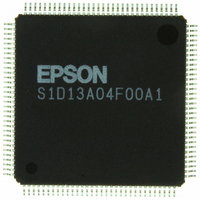
S1D13A04F00A Epson Electronics America Inc-Semiconductor Div, S1D13A04F00A Datasheet - Page 536

S1D13A04F00A
Manufacturer Part Number
S1D13A04F00A
Description
IC LCD COMPANION 160KB 128-TQFP
Manufacturer
Epson Electronics America Inc-Semiconductor Div
Specifications of S1D13A04F00A
Display Type
LCD
Voltage - Supply
1.8 V ~ 2.75 V
Mounting Type
Surface Mount
Package / Case
125-TQFP, 125-VQFP
Lead Free Status / RoHS Status
Lead free / RoHS Compliant
Current - Supply
-
Operating Temperature
-
Interface
-
Configuration
-
Digits Or Characters
-
Other names
S1D13A04F00A100
S1D13A04F00A100
S1D13A04F00A100
Available stocks
Company
Part Number
Manufacturer
Quantity
Price
Company:
Part Number:
S1D13A04F00A
Manufacturer:
Epson Electronics America Inc-Semiconductor Div
Quantity:
10 000
Company:
Part Number:
S1D13A04F00A1
Manufacturer:
EPSON
Quantity:
816
Part Number:
S1D13A04F00A1
Manufacturer:
EPSON/爱普生
Quantity:
20 000
Company:
Part Number:
S1D13A04F00A100
Manufacturer:
OSRAM
Quantity:
4 600
- Current page: 536 of 598
- Download datasheet (6Mb)
Page 12
3.2 Host Bus Interface Signals
S1D13A04
X37A-G-010-01
The Host Bus Interface requires the following signals.
• CLKI is a clock input which is required by the S1D13A04 Host Bus Interface as a
• The address inputs AB[17:0] connect directly to the MCF5307 address bus (A[17:0]).
• DB[7:0] connects D[23:16] (the MCF5307 low order byte). DB[15:8] connects to
• Chip Select (CS#) must be driven low by CS4 whenever the S1D13A04 is accessed by
• M/R# (memory/register) selects between memory or register accesses. This signal is
• WE0# connects to BWE0 (the low byte enable signal from the MCF5307) and must be
• WE1# connects to BWE1 (the high byte enable signal from the MCF5307) and must be
• RD# and RD/WR# are read enables for the low-order and high-order bytes, respectively.
• WAIT# connects to TA and is a signal which is output from the S1D13A04 that indi-
• The Bus Status (BS#) signal is not used in the bus interface for Generic #1 mode and
source for its internal bus and memory clocks. This clock is typically driven by the host
CPU system clock. For this example, BCLK0 from the Motorola MCF5307 is used for
CLKI.
D[31:24] (the MCF5307 high order byte). CNF4 must be set to select big endian mode.
the Motorola MCF5307.
generated by the external address decode circuitry. For this example, M/R# is connected
to address line A18, allowing system address A18 to select between memory or register
accesses.
driven low when the MCF5307 is writing the low byte to the S1D13A04.
driven low when the MCF5307 is writing the high byte to the S1D13A04.
Both signals are driven low by OE when the Motorola MCF5307 is reading data from
the S1D13A04.
cates the host CPU must wait until data is ready (read cycle) or accepted (write cycle) on
the host bus. Since host CPU accesses to the S1D13A04 may occur asynchronously to
the display update, it is possible that contention may occur in accessing the S1D13A04
internal registers and/or refresh memory. The WAIT# line resolves these contentions by
forcing the host to wait until the resource arbitration is complete. This signal is active
low and may need to be inverted if the host CPU wait state signal is active high.
must be tied high to IO V
DD
.
Interfacing to the Motorola MCF5307 "ColdFire" Microprocessor
Epson Research and Development
Vancouver Design Center
Issue Date: 01/10/12
Related parts for S1D13A04F00A
Image
Part Number
Description
Manufacturer
Datasheet
Request
R

Part Number:
Description:
IC CONTROLLER CRT/LCD/TV 128-QFP
Manufacturer:
Epson Electronics America Inc-Semiconductor Div
Part Number:
Description:
IC GRAPHIC LCD CTRLR 256-PBGA
Manufacturer:
Epson Electronics America Inc-Semiconductor Div
Datasheet:
Part Number:
Description:
MEMORY CARD 2M STATIC RAM
Manufacturer:
Epson Electronics America Inc-Semiconductor Div
Part Number:
Description:
IC CTRLR/PHY USB OTG 64-QFP
Manufacturer:
Epson Electronics America Inc-Semiconductor Div
Part Number:
Description:
IC CONTROLLER USB 2.0 64-QFP
Manufacturer:
Epson Electronics America Inc-Semiconductor Div

Part Number:
Description:
IC PHY CONT 2PORT 1394A 100-QFP
Manufacturer:
Epson Electronics America Inc-Semiconductor Div
Part Number:
Description:
IC LINK CTRLR 1394 IDE-33 184QFP
Manufacturer:
Epson Electronics America Inc-Semiconductor Div
Part Number:
Description:
IC LINK CTRLR 1394 IDE-66 184QFP
Manufacturer:
Epson Electronics America Inc-Semiconductor Div

Part Number:
Description:
IC LINK CTRLR 1394 IDE100 100QFP
Manufacturer:
Epson Electronics America Inc-Semiconductor Div

Part Number:
Description:
IC LINK CTRLR/PHY 1394 100-QFP
Manufacturer:
Epson Electronics America Inc-Semiconductor Div
Part Number:
Description:
IC CTRLR/PHY USB 2.0 64-QFP
Manufacturer:
Epson Electronics America Inc-Semiconductor Div

Part Number:
Description:
IC CTRLR/PHY USB 2.0 100-QFP
Manufacturer:
Epson Electronics America Inc-Semiconductor Div
Part Number:
Description:
IC CHARGE CTRLR LI-ION 24-SSOP
Manufacturer:
Epson Electronics America Inc-Semiconductor Div
Part Number:
Description:
IC BATTERY LEAK PREVENTION SOT89
Manufacturer:
Epson Electronics America Inc-Semiconductor Div
Part Number:
Description:
IC BATTERY LEAK PREVENTION SOT89
Manufacturer:
Epson Electronics America Inc-Semiconductor Div


