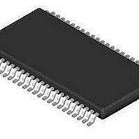
PCA85162T/Q900/1,1 NXP Semiconductors, PCA85162T/Q900/1,1 Datasheet - Page 6

PCA85162T/Q900/1,1
Manufacturer Part Number
PCA85162T/Q900/1,1
Description
IC INTERFACE
Manufacturer
NXP Semiconductors
Datasheet
1.PCA85162TQ90011.pdf
(42 pages)
Specifications of PCA85162T/Q900/1,1
Package / Case
48-TSSOP
Display Type
LCD
Configuration
32 Segment
Interface
I²C
Current - Supply
80µA
Voltage - Supply
1.8 V ~ 5.5 V
Operating Temperature
-40°C ~ 95°C
Mounting Type
Surface Mount
Number Of Digits
16
Number Of Segments
32
Maximum Clock Frequency
4800 Hz
Operating Supply Voltage
1.8 V to 5.5 V
Maximum Power Dissipation
400 mW
Maximum Operating Temperature
+ 95 C
Attached Touch Screen
No
Maximum Supply Current
20 uA
Minimum Operating Temperature
- 40 C
Lead Free Status / RoHS Status
Lead free / RoHS Compliant
Digits Or Characters
-
Lead Free Status / Rohs Status
Details
Other names
568-5119-2
NXP Semiconductors
PCA85162_1
Product data sheet
7.2 LCD bias generator
7.3 LCD voltage selector
Remark: Do not transfer data on the I
the reset action to complete.
Fractional LCD biasing voltages are obtained from an internal voltage divider of the three
series resistors connected between V
switch if the
The LCD voltage selector coordinates the multiplexing of the LCD in accordance with the
selected LCD drive configuration. The operation of the voltage selector is controlled by the
mode-set command from the command decoder. The biasing configurations that apply to
the preferred modes of operation, together with the biasing characteristics as functions of
V
Table 5.
A practical value for V
threshold voltage (V
the static drive mode a suitable choice is V
Multiplex drive modes of 1:3 and 1:4 with
hence the contrast ratios are smaller.
Bias is calculated by
The RMS on-state voltage (V
where the values for n are
V
LCD drive
mode
static
1:2 multiplex 2
1:2 multiplex 2
1:3 multiplex 3
1:4 multiplex 4
LCD
•
on RMS
a = 1 for
a = 2 for
n = 1 for static drive mode
n = 2 for 1:2 multiplex drive mode
n = 3 for 1:3 multiplex drive mode
n = 4 for 1:4 multiplex drive mode
(
Display is disabled
and the resulting discrimination ratios (D) are given in
)
=
Biasing characteristics
1
1
⁄
⁄
V
2
3
1
LCD
⁄
2
Number of:
Backplanes Levels
1
bias
bias
bias voltage level for the 1:2 multiplex configuration is selected.
All information provided in this document is subject to legal disclaimers.
----------------------------- -
n
a
2
×
th
+
(
------------ -
1
), typically when the LCD exhibits approximately 10 % contrast. In
1
LCD
2a
1
+
Rev. 01 — 19 April 2010
+
a
+
a
is determined by equating V
)
, where the values for a are
n
2
3
4
4
4
2
on(RMS)
LCD bias
configuration
static
1
1
1
1
⁄
⁄
⁄
⁄
) for the LCD is calculated with
2
3
3
3
LCD
2
C-bus for at least 1 ms after a power-on to allow
and V
1
Universal LCD driver for low multiplex rates
⁄
LCD
2
bias are possible but the discrimination and
> 3V
SS
. The center resistor is bypassed by
th
0
0.354
0.333
0.333
0.333
V
------------------------ -
.
off RMS
V
off(RMS)
LCD
(
Table
)
with a defined LCD
1
0.791
0.745
0.638
0.577
V
----------------------- -
on RMS
V
5.
(
LCD
Equation
PCA85162
)
© NXP B.V. 2010. All rights reserved.
∞
2.236
2.236
1.915
1.732
D
=
1:
------------------------ -
V
V
off RMS
on RMS
(
(
6 of 42
)
(1)
)


