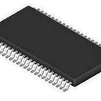
PCA85162T/Q900/1,1 NXP Semiconductors, PCA85162T/Q900/1,1 Datasheet - Page 28

PCA85162T/Q900/1,1
Manufacturer Part Number
PCA85162T/Q900/1,1
Description
IC INTERFACE
Manufacturer
NXP Semiconductors
Datasheet
1.PCA85162TQ90011.pdf
(42 pages)
Specifications of PCA85162T/Q900/1,1
Package / Case
48-TSSOP
Display Type
LCD
Configuration
32 Segment
Interface
I²C
Current - Supply
80µA
Voltage - Supply
1.8 V ~ 5.5 V
Operating Temperature
-40°C ~ 95°C
Mounting Type
Surface Mount
Number Of Digits
16
Number Of Segments
32
Maximum Clock Frequency
4800 Hz
Operating Supply Voltage
1.8 V to 5.5 V
Maximum Power Dissipation
400 mW
Maximum Operating Temperature
+ 95 C
Attached Touch Screen
No
Maximum Supply Current
20 uA
Minimum Operating Temperature
- 40 C
Lead Free Status / RoHS Status
Lead free / RoHS Compliant
Digits Or Characters
-
Lead Free Status / Rohs Status
Details
Other names
568-5119-2
NXP Semiconductors
11. Dynamic characteristics
Table 17.
V
[1]
[2]
[3]
PCA85162_1
Product data sheet
Symbol
Clock
f
f
f
t
t
Synchronization
t
t
t
I
Pin SCL
f
t
t
Pin SDA
t
t
Pins SCL and SDA
t
t
t
t
t
t
C
t
clk(int)
clk(ext)
fr
clk(H)
clk(L)
PD(SYNC_N)
SYNC_NL
PD(drv)
2
SCL
LOW
HIGH
SU;DAT
HD;DAT
BUF
SU;STO
HD;STA
SU;STA
r
f
w(spike)
DD
C-bus
b
= 1.8 V to 5.5 V; V
Typical output duty factor: 50 % measured at the CLK output pin.
Not tested in production.
All timing values are valid within the operating supply voltage and ambient temperature range and are referenced to V
input voltage swing of V
[3]
Dynamic characteristics
Parameter
internal clock frequency
external clock frequency
frame frequency
HIGH-level clock time
LOW-level clock time
SYNC propagation delay
SYNC LOW time
driver propagation delay
SCL clock frequency
LOW period of the SCL clock
HIGH period of the SCL clock
data set-up time
data hold time
bus free time between a STOP and
START condition
set-up time for STOP condition
hold time (repeated) START condition
set-up time for a repeated START
condition
rise time of both SDA and SCL signals f
fall time of both SDA and SCL signals
capacitive load for each bus line
spike pulse width
SS
SS
= 0 V; V
to V
DD
LCD
.
= 2.5 V to 8.0 V; T
All information provided in this document is subject to legal disclaimers.
Rev. 01 — 19 April 2010
Conditions
internal clock
external clock
V
f
on the I
SCL
SCL
LCD
amb
= 400 kHz
< 125 kHz
= 5 V
=
2
−
C-bus
40
°
C to +95
[1]
[2]
Universal LCD driver for low multiplex rates
°
C; unless otherwise specified.
Min
1920
960
80
40
60
60
-
1
-
-
1.3
0.6
100
0
1.3
0.6
0.6
0.6
-
-
-
-
-
Typ
2640
-
110
-
-
-
30
-
-
-
-
-
-
-
-
-
-
-
-
-
-
-
-
PCA85162
Max
3600
4800
150
200
-
-
-
-
30
400
-
-
-
-
-
-
-
-
0.3
400
50
0.3
1.0
© NXP B.V. 2010. All rights reserved.
IL
and V
IH
Unit
Hz
Hz
Hz
Hz
μs
μs
ns
μs
μs
kHz
μs
μs
ns
ns
μs
μs
μs
μs
μs
μs
μs
pF
ns
28 of 42
with an


