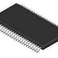
PCA85162T/Q900/1,1 NXP Semiconductors, PCA85162T/Q900/1,1 Datasheet - Page 13

PCA85162T/Q900/1,1
Manufacturer Part Number
PCA85162T/Q900/1,1
Description
IC INTERFACE
Manufacturer
NXP Semiconductors
Datasheet
1.PCA85162TQ90011.pdf
(42 pages)
Specifications of PCA85162T/Q900/1,1
Package / Case
48-TSSOP
Display Type
LCD
Configuration
32 Segment
Interface
I²C
Current - Supply
80µA
Voltage - Supply
1.8 V ~ 5.5 V
Operating Temperature
-40°C ~ 95°C
Mounting Type
Surface Mount
Number Of Digits
16
Number Of Segments
32
Maximum Clock Frequency
4800 Hz
Operating Supply Voltage
1.8 V to 5.5 V
Maximum Power Dissipation
400 mW
Maximum Operating Temperature
+ 95 C
Attached Touch Screen
No
Maximum Supply Current
20 uA
Minimum Operating Temperature
- 40 C
Lead Free Status / RoHS Status
Lead free / RoHS Compliant
Digits Or Characters
-
Lead Free Status / Rohs Status
Details
Other names
568-5119-2
NXP Semiconductors
PCA85162_1
Product data sheet
7.5.1 Internal clock
7.5.2 External clock
7.5 Oscillator
7.6 Timing
7.7 Display register
7.8 Segment outputs
7.9 Backplane outputs
The internal logic of the PCA85162 and its LCD drive signals are timed either by its
internal oscillator or by an external clock. The internal oscillator is enabled by connecting
pin OSC to pin V
as the clock signal for several PCA85162 in the system that are connected in cascade.
Pin CLK is enabled as an external clock input by connecting pin OSC to V
frame signal frequency is determined by the clock frequency (f
A clock signal must always be supplied to the device; removing the clock may freeze the
LCD in a DC state, which is not suitable for the liquid crystal.
The PCA85162 timing controls the internal data flow of the device. This includes the
transfer of display data from the display RAM to the display segment outputs. In cascaded
applications, the correct timing relationship between each PCA85162 in the system is
maintained by the synchronization signal at pin SYNC. The timing also generates the LCD
frame signal whose frequency is derived from the clock frequency. The frame signal
frequency is a fixed division of the clock frequency from either the internal or an external
clock:
The display register holds the display data while the corresponding multiplex signals are
generated.
The LCD drive section includes 32 segment outputs S0 to S31 which should be
connected directly to the LCD. The segment output signals are generated in accordance
with the multiplexed backplane signals and with data residing in the display register. When
less than 32 segment outputs are required, the unused segment outputs should be left
open-circuit.
The LCD drive section includes four backplane outputs BP0 to BP3 which must be
connected directly to the LCD. The backplane output signals are generated in accordance
with the selected LCD drive mode. If less than four backplane outputs are required, the
unused outputs can be left open-circuit.
•
•
In 1:3 multiplex drive mode, BP3 carries the same signal as BP1, therefore these two
adjacent outputs can be tied together to give enhanced drive capabilities.
In 1:2 multiplex drive mode, BP0 and BP2, BP1 and BP3 all carry the same signals
and may also be paired to increase the drive capabilities.
f
fr
=
f
-------
24
clk
All information provided in this document is subject to legal disclaimers.
SS
. If the internal oscillator is used, the output from pin CLK can be used
Rev. 01 — 19 April 2010
Universal LCD driver for low multiplex rates
clk
).
PCA85162
© NXP B.V. 2010. All rights reserved.
DD
. The LCD
13 of 42


