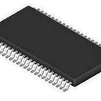
PCA85162T/Q900/1,1 NXP Semiconductors, PCA85162T/Q900/1,1 Datasheet - Page 19

PCA85162T/Q900/1,1
Manufacturer Part Number
PCA85162T/Q900/1,1
Description
IC INTERFACE
Manufacturer
NXP Semiconductors
Datasheet
1.PCA85162TQ90011.pdf
(42 pages)
Specifications of PCA85162T/Q900/1,1
Package / Case
48-TSSOP
Display Type
LCD
Configuration
32 Segment
Interface
I²C
Current - Supply
80µA
Voltage - Supply
1.8 V ~ 5.5 V
Operating Temperature
-40°C ~ 95°C
Mounting Type
Surface Mount
Number Of Digits
16
Number Of Segments
32
Maximum Clock Frequency
4800 Hz
Operating Supply Voltage
1.8 V to 5.5 V
Maximum Power Dissipation
400 mW
Maximum Operating Temperature
+ 95 C
Attached Touch Screen
No
Maximum Supply Current
20 uA
Minimum Operating Temperature
- 40 C
Lead Free Status / RoHS Status
Lead free / RoHS Compliant
Digits Or Characters
-
Lead Free Status / Rohs Status
Details
Other names
568-5119-2
NXP Semiconductors
PCA85162_1
Product data sheet
7.16.3 System configuration
7.16.4 Acknowledge
A device generating a message is a transmitter, a device receiving a message is the
receiver. The device that controls the message is the master and the devices which are
controlled by the master are the slaves (see
The number of data bytes transferred between the START and STOP conditions from
transmitter to receiver is unlimited. Each byte of eight bits is followed by an acknowledge
cycle.
Acknowledgement on the I
Fig 12. Definition of START and STOP conditions
Fig 13. System configuration
•
•
•
•
A slave receiver, which is addressed, must generate an acknowledge after the
reception of each byte.
A master receiver must generate an acknowledge after the reception of each byte that
has been clocked out of the slave transmitter.
The device that acknowledges must pull-down the SDA line during the acknowledge
clock pulse, so that the SDA line is stable LOW during the HIGH period of the
acknowledge related clock pulse (set-up and hold times must be taken into
consideration).
A master receiver must signal an end of data to the transmitter by not generating an
acknowledge on the last byte that has been clocked out of the slave. In this event, the
transmitter must leave the data line HIGH to enable the master to generate a STOP
condition.
SCL
SDA
SDA
SCL
TRANSMITTER/
RECEIVER
MASTER
START condition
All information provided in this document is subject to legal disclaimers.
S
Rev. 01 — 19 April 2010
RECEIVER
2
C-bus is illustrated in
SLAVE
TRANSMITTER/
RECEIVER
Universal LCD driver for low multiplex rates
SLAVE
Figure
Figure
13).
TRANSMITTER
14.
MASTER
STOP condition
PCA85162
P
TRANSMITTER/
© NXP B.V. 2010. All rights reserved.
RECEIVER
MASTER
mbc622
mga807
SDA
SCL
19 of 42


