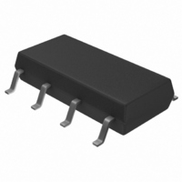
FSDM0365RL Fairchild Semiconductor, FSDM0365RL Datasheet - Page 16

FSDM0365RL
Manufacturer Part Number
FSDM0365RL
Description
IC SWIT PWM GREEN CM OVP HV 8SOP
Manufacturer
Fairchild Semiconductor
Datasheet
1.FSDL0365RL.pdf
(22 pages)
Specifications of FSDM0365RL
Output Isolation
Isolated
Frequency Range
61 ~ 73kHz
Voltage - Input
8 ~ 20 V
Voltage - Output
650V
Power (watts)
30W
Operating Temperature
25°C ~ 140°C
Package / Case
8-SOP, 8-LSOP
Lead Free Status / RoHS Status
Lead free / RoHS Compliant
Other names
FSDM0365RL_NL
FSDM0365RL_NL
FSDM0365RL_NL
Available stocks
Company
Part Number
Manufacturer
Quantity
Price
Company:
Part Number:
FSDM0365RLX
Manufacturer:
FREESCALE
Quantity:
769
Company:
Part Number:
FSDM0365RLX
Manufacturer:
Fairchi/ON
Quantity:
4 000
FSDL0365RN, FSDM0365RN
Typical application circuit
1. Set Top Box Example Circuit (20W Output Power)
Multiple Output, 20W, 85-265VAC Input Power supply:
Figure 15 shows a multiple output supply typical for high
end set-top boxes containing high capacity hard disks for
recording or LIPS(LCD Inverter Power Supply) for 15"
LCD monitor. The supply delivers an output power of 20W
cont./24 W peak (thermally limited) from an input voltage of
85 to 265 VAC. Efficiency at 20W, 85VAC is ≥75%.
The 3.3 V and 5 V outputs are regulated to ±5% without the
need for secondary linear regulators. DC stacking (the sec-
ondary winding reference for the other output voltages is
connected to the anode of D15. For more accuracy, connec-
tion to the cathode of D15 will be better.) is used to minimize
the voltage error for the higher voltage outputs. Due to the
high ambient operating temperature requirement typical of a
set-top box (60 °C) the FSDL0165RN is used to reduce con-
duction losses without a heatsink. Resistor R5 sets the device
current limit to limit overload power.
Leakage inductance clamping is provided by R1 and C8,
keeping the DRAIN voltage below 650 V under all condi-
tions. Resistor R1 and capacitor C8 are selected such that R1
dissipates power to prevent rising of DRAIN Voltage caused
by leakage inductance. The frequency modulation feature of
FSDL0165RN allows the circuit shown to meet CISPR2AB
with simple EMI filtering (C1, LF1 and C2) and the output
grounded. The secondaries are rectified and smoothed by
D12, D13, D14,and D15. Diode D15 for the 3.4V output is a
Schottky diode to maximize efficiency. Diode D14 for the 5
V output is a PN type to center the 5 V output at 5 V. The 3.3
V and 5 V output voltage require two capacitors in parallel to
meet the ripple current requirement. Switching noise filter-
16
~275VAC
85VAC
PERFORMANCE SUMMARY
Output Power:
Regulation
3.3V:
5.0V:
17.0V:
23.0:
Efficiency:
No load Consumption:
0.12W at 230Vac
2A/250V
FUSE
100pF
/400V
C1
40mH
LF1
100pF
/400V
C2
Figure15. 20W multiple power supply using FSDM0365RN
≥75%
±7%
±5%
±5%
±7%
20W
KBP06M
GreenFPS
400V
/47u
C7
ZD1
19V
D
47uF
G Vcc Vfb
1
50V
C6
FSDM0365RN
D
33n
50V
C9
56K/1/
R3
4W
D
ZD2
19V
start
I_pk
5
6kR
R5
47K
R1
UF4004
D6
PC817
6.8n/1k
C8
V
UF4007
D5
ing is provided by L3, L2 and L1. Resistor R15 prevents
peak charging of the lightly loaded 23V output. The outputs
are regulated by the reference (TL431) voltage in secondary.
Both the 3.3 V and 5 V outputs are sensed via R13 and R14.
Resistor R22 provides bias for TL431and R21 sets the over-
all DC gain. Resistor R21, C209, R14 and R13 provide loop
compensation.
30R
R4
Q1
FOD2741A
4
5
1
3
10
12
11
6
8
EGP20D
D12
EGP20D
PC817
TL431AZ
EGP20D
SB360
D13
330R
D14
D15
R21
20R
R15
R15
1000uF
0.1uF/mon
1000uF
C17
C15
C13
C11
1KR
/16V
R22
/16V
100uF
470uF
olithic
/50V
/35V
L1
6.9K
C209
L3
L2
800R
R14
R12
1.5K
470uF
470uF
R13
/10V
C12
2.7K
/10V
C14
C16
220uF
100uF
/35V
/50V
R19
R20
0.005~0.45A
0.01~0.5A
0.4~1.4A
+17.0V
+23.0V
+5.0V
+3.3V
0.2~0.85A


