EPC4QC100N Altera, EPC4QC100N Datasheet - Page 19
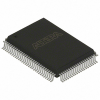
EPC4QC100N
Manufacturer Part Number
EPC4QC100N
Description
IC CONFIG DEVICE 4MBIT 100-PQFP
Manufacturer
Altera
Series
EPCr
Specifications of EPC4QC100N
Programmable Type
In System Programmable
Memory Size
4Mb
Voltage - Supply
3 V ~ 3.6 V
Operating Temperature
0°C ~ 70°C
Package / Case
100-MQFP, 100-PQFP
Memory Type
Flash
Clock Frequency
66.7MHz
Supply Voltage Range
3V To 3.6V
Memory Case Style
QFP
No. Of Pins
100
Operating Temperature Range
0°C To +70°C
Access Time
90ns
Rohs Compliant
Yes
Lead Free Status / RoHS Status
Lead free / RoHS Compliant
Other names
544-1378
EPC4QC100N
EPC4QC100N
Available stocks
Company
Part Number
Manufacturer
Quantity
Price
Company:

Part Number:
EPC4QC100N
Manufacturer:
ALTERA
Quantity:
25
Company:
Part Number:
EPC4QC100N
Manufacturer:
Altera
Quantity:
135
Company:
Part Number:
EPC4QC100N
Manufacturer:
ALTERA32EOL
Quantity:
135


Chapter 1: Enhanced Configuration Devices (EPC4, EPC8, and EPC16) Data Sheet
Functional Description
Programmable Configuration Clock
© December 2009 Altera Corporation
f
Table 1–6. Stratix Compression Ratios
The configuration clock (DCLK) speed is user programmable. One of two clock sources
can be used to synthesize the configuration clock; a programmable oscillator or an
external clock input pin (EXCLK). The configuration clock frequency can be further
synthesized using the clock divider circuitry. This clock can be divided by the N
counter to generate your DCLK output. The N divider supports all integer dividers
between 1 and 16, as well as a 1.5 divider and a 2.5 divider. The duty cycle for all clock
divisions other than non-integer divisions is 50% (for the non-integer dividers, the
duty cycle will not be 50%). Refer to
divider unit.
Figure 1–5. Clock Divider Unit
The DCLK frequency is limited by the maximum DCLK frequency the FPGA supports.
The maximum DCLK input frequency supported by the FGPA is specified in the
appropriate FPGA family chapter in the
Logic Utilization
Compression Ratio
% Size Reduction
Note to
(1) These numbers are preliminary. They are intended to serve as a guideline, not a specification.
Table
(Up to 100 MHz)
External Clock
1–6:
Item
10 MHz
33 MHz
50 MHz
66 MHz
Internal Oscillator
(Note 1)
Figure 1–5
Configuration Device
Minimum
Configuration
98%
47%
1.9
Clock Divider Unit
for a block diagram of the clock
Configuration Handbook (Complete Two-Volume Set)
Divide
by N
Handbook.
Average
64%
57%
2.3
DCLK
1–19
Related parts for EPC4QC100N
Image
Part Number
Description
Manufacturer
Datasheet
Request
R

Part Number:
Description:
Sram-based LUT Devices
Manufacturer:
Altera Corporation
Datasheet:

Part Number:
Description:
(EPC4 / EPC8 / EPC16) Enhanced Configuration Devices
Manufacturer:
Altera
Datasheet:

Part Number:
Description:
CYCLONE II STARTER KIT EP2C20N
Manufacturer:
Altera
Datasheet:
Part Number:
Description:
CPLD, EP610 Family, ECMOS Process, 300 Gates, 16 Macro Cells, 16 Reg., 16 User I/Os, 5V Supply, 35 Speed Grade, 24DIP
Manufacturer:
Altera Corporation
Datasheet:
Part Number:
Description:
CPLD, EP610 Family, ECMOS Process, 300 Gates, 16 Macro Cells, 16 Reg., 16 User I/Os, 5V Supply, 15 Speed Grade, 24DIP
Manufacturer:
Altera Corporation
Datasheet:
Part Number:
Description:
Manufacturer:
Altera Corporation
Datasheet:
Part Number:
Description:
CPLD, EP610 Family, ECMOS Process, 300 Gates, 16 Macro Cells, 16 Reg., 16 User I/Os, 5V Supply, 30 Speed Grade, 24DIP
Manufacturer:
Altera Corporation
Datasheet:
Part Number:
Description:
High-performance, low-power erasable programmable logic devices with 8 macrocells, 10ns
Manufacturer:
Altera Corporation
Datasheet:
Part Number:
Description:
High-performance, low-power erasable programmable logic devices with 8 macrocells, 7ns
Manufacturer:
Altera Corporation
Datasheet:
Part Number:
Description:
Classic EPLD
Manufacturer:
Altera Corporation
Datasheet:
Part Number:
Description:
High-performance, low-power erasable programmable logic devices with 8 macrocells, 10ns
Manufacturer:
Altera Corporation
Datasheet:
Part Number:
Description:
Manufacturer:
Altera Corporation
Datasheet:
Part Number:
Description:
Manufacturer:
Altera Corporation
Datasheet: