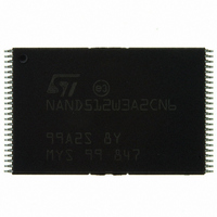
NAND512W3A2CN6E NUMONYX, NAND512W3A2CN6E Datasheet - Page 34

NAND512W3A2CN6E
Manufacturer Part Number
NAND512W3A2CN6E
Description
IC FLASH 512MBIT 48TSOP
Manufacturer
NUMONYX
Datasheet
1.NAND512R3A2CZA6E.pdf
(55 pages)
Specifications of NAND512W3A2CN6E
Format - Memory
FLASH
Memory Type
FLASH - Nand
Memory Size
512M (64M x 8)
Interface
Parallel
Voltage - Supply
2.7 V ~ 3.6 V
Operating Temperature
-40°C ~ 85°C
Package / Case
48-TSOP
Cell Type
NAND
Density
512Mb
Access Time (max)
12us
Interface Type
Parallel
Boot Type
Not Required
Address Bus
26b
Operating Supply Voltage (typ)
3/3.3V
Operating Temp Range
-40C to 85C
Package Type
TSOP
Program/erase Volt (typ)
2.7 to 3.6V
Sync/async
Asynchronous
Operating Temperature Classification
Industrial
Operating Supply Voltage (min)
2.7V
Operating Supply Voltage (max)
3.6V
Word Size
8b
Number Of Words
64M
Supply Current
20mA
Mounting
Surface Mount
Pin Count
48
Lead Free Status / RoHS Status
Lead free / RoHS Compliant
Speed
-
Lead Free Status / RoHS Status
Lead free / RoHS Compliant, Compliant
Available stocks
Company
Part Number
Manufacturer
Quantity
Price
Company:
Part Number:
NAND512W3A2CN6E
Manufacturer:
MICRON
Quantity:
1 500
Part Number:
NAND512W3A2CN6E
Manufacturer:
ST
Quantity:
20 000
Program and erase times and endurance cycles
8
9
34/55
Program and erase times and endurance cycles
The program and erase times and the number of program/erase cycles per block are shown
in
Table 14.
Maximum ratings
Stressing the device above the ratings listed in
cause permanent damage to the device. These are stress ratings only and operation of the
device at these or any other conditions above those indicated in the operating sections of
this specification is not implied. Exposure to absolute maximum rating conditions for
extended periods may affect device reliability.
Table 15.
1. Minimum voltage may undershoot to –2 V for less than 20 ns during transitions on input and I/O pins.
Page program time
Block erase time
Program/erase cycles per block (with ECC)
Data retention
Table
Maximum voltage may overshoot to V
Symbol
T
T
V
T
V
LEAD
BIAS
IO
STG
DD
14.
(1)
Program, erase times and program erase endurance cycles
Absolute maximum ratings
Parameters
Temperature under bias
Storage temperature
Lead temperature during soldering
Input or output voltage
Supply voltage
Parameter
DD
+ 2 V for less than 20 ns during transitions on I/O pins.
1.8 V devices
1.8 V devices
3 V devices
3 V devices
100,000
Min
10
Table 15: Absolute maximum
NAND flash
– 0.6
– 0.6
– 0.6
– 0.6
Typ
200
– 50
– 65
Min
2
Value
Max
500
Max
125
150
260
2.7
4.6
2.7
4.6
3
NAND512-A2C
ratings, may
cycles
years
Unit
ms
Unit
µs
°C
°C
°C
V
V
V
V


