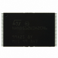
NAND512W3A2CN6E NUMONYX, NAND512W3A2CN6E Datasheet - Page 15

NAND512W3A2CN6E
Manufacturer Part Number
NAND512W3A2CN6E
Description
IC FLASH 512MBIT 48TSOP
Manufacturer
NUMONYX
Datasheet
1.NAND512R3A2CZA6E.pdf
(55 pages)
Specifications of NAND512W3A2CN6E
Format - Memory
FLASH
Memory Type
FLASH - Nand
Memory Size
512M (64M x 8)
Interface
Parallel
Voltage - Supply
2.7 V ~ 3.6 V
Operating Temperature
-40°C ~ 85°C
Package / Case
48-TSOP
Cell Type
NAND
Density
512Mb
Access Time (max)
12us
Interface Type
Parallel
Boot Type
Not Required
Address Bus
26b
Operating Supply Voltage (typ)
3/3.3V
Operating Temp Range
-40C to 85C
Package Type
TSOP
Program/erase Volt (typ)
2.7 to 3.6V
Sync/async
Asynchronous
Operating Temperature Classification
Industrial
Operating Supply Voltage (min)
2.7V
Operating Supply Voltage (max)
3.6V
Word Size
8b
Number Of Words
64M
Supply Current
20mA
Mounting
Surface Mount
Pin Count
48
Lead Free Status / RoHS Status
Lead free / RoHS Compliant
Speed
-
Lead Free Status / RoHS Status
Lead free / RoHS Compliant, Compliant
Available stocks
Company
Part Number
Manufacturer
Quantity
Price
Company:
Part Number:
NAND512W3A2CN6E
Manufacturer:
MICRON
Quantity:
1 500
Part Number:
NAND512W3A2CN6E
Manufacturer:
ST
Quantity:
20 000
NAND512-A2C
3.6
3.7
3.8
3.9
3.10
Read Enable (R)
The Read Enable, R, controls the sequential data output during read operations. Data is
valid t
column address counter by one.
Write Enable (W)
The Write Enable input, W, controls writing to the command interface, input address and
data latches. Both addresses and data are latched on the rising edge of Write Enable.
During power-up and power-down a recovery time of 10 µs (min) is required before the
command interface is ready to accept a command. It is recommended to keep Write Enable
High during the recovery time.
Write Protect (WP)
The Write Protect pin is an input that gives a hardware protection against unwanted program
or erase operations. When Write Protect is Low, V
program or erase operations.
It is recommended to keep the Write Protect pin Low, V
Ready/Busy (RB)
The Ready/Busy output, RB, is an open-drain output that can be used to identify if the P/E/R
controller is currently active.
When Ready/Busy is Low, V
operation completes Ready/Busy goes High, V
The use of an open-drain output allows the Ready/Busy pins from several memories to be
connected to a single pull-up resistor. A Low will then indicate that one, or more, of the
memories is busy.
During power-up and power-down a recovery time of 10 µs (min) is required before the
command interface is ready to accept a command. During the recovery time the RB signal is
Low, V
Refer to the
calculate the value of the pull-up resistor.
V
V
power supply for all operations (read, program and erase).
An internal voltage detector disables all functions whenever V
(see
operations during power-transitions.
Each device in a system should have V
widths should be sufficient to carry the required program and erase currents
DD
DD
provides the power supply to the internal core of the memory device. It is the main
Figure 36: Data
RLQV
supply voltage
OL
.
after the falling edge of R. The falling edge of R also increments the internal
Section 10.1: Ready/Busy signal electrical characteristics
protection) to protect the device from any involuntary program/erase
OL
, a read, program or erase operation is in progress. When the
DD
decoupled with a 0.1 µF capacitor. The PCB track
OH
.
IL
, the device does not accept any
IL
, during power-up and power-down.
DD
is below the V
for details on how to
Signal descriptions
LKO
threshold
15/55


