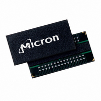
MT41J256M4HX-15E:D TR Micron Technology Inc, MT41J256M4HX-15E:D TR Datasheet - Page 44

MT41J256M4HX-15E:D TR
Manufacturer Part Number
MT41J256M4HX-15E:D TR
Description
IC DDR3 SDRAM 1GBIT 78FBGA
Manufacturer
Micron Technology Inc
Type
DDR3 SDRAMr
Specifications of MT41J256M4HX-15E:D TR
Format - Memory
RAM
Memory Type
DDR3 SDRAM
Memory Size
1G (256M x 4)
Speed
667MHz
Interface
Parallel
Voltage - Supply
1.425 V ~ 1.575 V
Operating Temperature
0°C ~ 95°C
Package / Case
78-FBGA
Organization
256Mx4
Density
1Gb
Address Bus
17b
Maximum Clock Rate
1.333GHz
Operating Supply Voltage (typ)
1.5V
Package Type
FBGA
Operating Temp Range
0C to 95C
Operating Supply Voltage (max)
1.575V
Operating Supply Voltage (min)
1.425V
Supply Current
220mA
Pin Count
78
Mounting
Surface Mount
Operating Temperature Classification
Commercial
Lead Free Status / RoHS Status
Lead free / RoHS Compliant
- Current page: 44 of 181
- Download datasheet (9Mb)
Table 25:
Figure 20: Single-Ended Requirements for Differential Signals
PDF: 09005aef826aa906/Source: 09005aef82a357c3
1Gb_DDR3_3.fm - Rev. F 11/08 EN
Parameter/Condition
Differential input voltage
Differential input midpoint voltage
Differential input voltage logic high
Differential input voltage logic low
Differential input crossing voltage relative
to V
Differential input crossing voltage relative
to V
DD
DD
/2 for CK, CK#
/2 for DQS, DQS#
Differential Input Operating Conditions (CK, CK# and DQS, DQS#)
All voltages are referenced to V
Notes:
1. V
2. The typical value of V
3. Reference is V
4. Clock is referenced to V
5. Differential input slew rate = 2 V/ns.
6. The V
V
DD
the true input (CK, DQS) level and V
V
and V
ferential input signals must cross.
extended range is only allowed when the following conditions are met: The single-ended
input signals are monotonic, have the single-ended swing V
±250mV, and the differential slew rate of CK, CK# is greater than 3 V/ns.
V
/2 or V
MP
MP
V
V
DD
V
SS
SEL
SEH
(
(
or V
DC
DC
or V
IX
(MAX)
IX
(MIN)
DD
) specifies the input differential common mode voltage (V
) is expected to be about 0.5 × V
(
extended range (±175mV) is allowed only for the clock. Additionally, the V
DD
AC
Q/2
SS
Q
Q
) is expected to track variations in V
REF
SS
CA(
Symbol
V
V
V
MP
IHDIFF
DC
ILDIFF
V
V
IX
IN
IX
(
) for clock and for V
DC
(
DD
AC
)
) is expected to be about 0.5 × V
and V
44
V
SEH
SS
. Data strobe is referenced to V
V
V
V
CP
REF
REF
REF
V
SS
is the complementary input (CK#, DQS#) level.
Micron Technology, Inc., reserves the right to change products or specifications without notice.
DD
(
(
(
–400
Electrical Specifications – DC and AC
Min
Q - 400
650
200
DC
DC
DC
Q.
REF
) - 150
) - 175
) - 150
DQ(
CK or DQS
DD
1Gb: x4, x8, x16 DDR3 SDRAM
. V
DC
IX
) for strobe.
(
AC
V
V
V
V
SEL
) indicates the voltage at which dif-
REF
REF
REF
V
V
DD
DD
DD
(
(
(
SEL
Max
–200
DC
DC
DC
850
of the transmitting device,
+ 400
+ 400
, V
) + 150
) + 175
) + 150
©2006 Micron Technology, Inc. All rights reserved.
TR
SEH
DD
+ V
Q and V
of at least V
CP
)/2 where V
SS
Q.
Units
mV
mV
mV
mV
mV
mV
mV
DD
IX
/2
TR
is
Related parts for MT41J256M4HX-15E:D TR
Image
Part Number
Description
Manufacturer
Datasheet
Request
R

Part Number:
Description:
Manufacturer:
Micron Technology Inc
Datasheet:

Part Number:
Description:
Manufacturer:
Micron Technology Inc
Datasheet:

Part Number:
Description:
IC SDRAM 64MBIT 133MHZ 54TSOP
Manufacturer:
Micron Technology Inc
Datasheet:

Part Number:
Description:
IC SDRAM 64MBIT 5.5NS 86TSOP
Manufacturer:
Micron Technology Inc
Datasheet:

Part Number:
Description:
IC SDRAM 64MBIT 200MHZ 86TSOP
Manufacturer:
Micron Technology Inc
Datasheet:

Part Number:
Description:
IC SDRAM 64MBIT 133MHZ 54TSOP
Manufacturer:
Micron Technology Inc
Datasheet:

Part Number:
Description:
IC SDRAM 128MBIT 133MHZ 54TSOP
Manufacturer:
Micron Technology Inc
Datasheet:

Part Number:
Description:
IC SDRAM 256MBIT 133MHZ 90VFBGA
Manufacturer:
Micron Technology Inc
Datasheet:

Part Number:
Description:
IC SDRAM 128MBIT 133MHZ 54TSOP
Manufacturer:
Micron Technology Inc
Datasheet:

Part Number:
Description:
IC SDRAM 256MBIT 133MHZ 54TSOP
Manufacturer:
Micron Technology Inc
Datasheet:

Part Number:
Description:
IC DDR SDRAM 512MBIT 6NS 66TSOP
Manufacturer:
Micron Technology Inc
Datasheet:

Part Number:
Description:
IC SDRAM 128MBIT 167MHZ 86TSOP
Manufacturer:
Micron Technology Inc
Datasheet:

Part Number:
Description:
IC SDRAM 128MBIT 143MHZ 86TSOP
Manufacturer:
Micron Technology Inc
Datasheet:

Part Number:
Description:
SDRAM 256M-BIT 1.8V 54-PIN VFBGA
Manufacturer:
Micron Technology Inc
Datasheet:

Part Number:
Description:
IC SDRAM 128MBIT 143MHZ 86TSOP
Manufacturer:
Micron Technology Inc
Datasheet:


