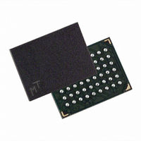
MT45W4MW16BCGB-701 WT Micron Technology Inc, MT45W4MW16BCGB-701 WT Datasheet - Page 7

MT45W4MW16BCGB-701 WT
Manufacturer Part Number
MT45W4MW16BCGB-701 WT
Description
IC PSRAM 64MBIT 70NS 54VFBGA
Manufacturer
Micron Technology Inc
Datasheet
1.MT45W4MW16BCGB-701_IT.pdf
(69 pages)
Specifications of MT45W4MW16BCGB-701 WT
Format - Memory
RAM
Memory Type
PSRAM (Page)
Memory Size
64M (4M x 16)
Speed
70ns
Interface
Parallel
Voltage - Supply
1.7 V ~ 1.95 V
Operating Temperature
-30°C ~ 85°C
Package / Case
54-VFBGA
Operating Temperature (max)
85C
Mounting
Surface Mount
Operating Temperature Classification
Commercial
Lead Free Status / RoHS Status
Lead free / RoHS Compliant
Table 1:
PDF: 09005aef8247bd51/Source: 09005aef8247bd83
64mb_burst_cr1_5_p25z_133mhz__2.fm - Rev. F 9/07 EN
G4, G3, H5, H4,
E3, H6, G2, H1,
H3, H2, D4, C4,
C3, B4, B3, A5,
D2, C2, C1, B1,
D3, E4, F4, F3,
G1, F1, F2, E2,
G6, F6, F5, E5,
D5, C6, C5, B6
Assignment
J4, J5, J6
VFBGA
A4, A3
A6
A2
G5
A1
D6
D1
B5
B2
E1
E6
J2
J3
J1
VFBGA Ball Descriptions
DQ[15:0]
Symbol
A[21:0]
ADV#
WAIT
V
V
WE#
OE#
UB#
CLK
CRE
RFU
CE#
LB#
V
V
CC
SS
CC
SS
Note:
Q
Q
Output
Output
Supply
Supply
Supply
Supply
Input/
Input
Input
Input
Input
Input
Input
Input
Input
Input
Type
The CLK and ADV# inputs can be tied to V
nous or page mode. WAIT will be asserted, but should be ignored during asynchronous
and page mode operations.
–
64Mb: 4 Meg x 16 Async/Page/Burst CellularRAM 1.5 Memory
Description
Address inputs: Inputs for addresses during READ and WRITE operations.
Addresses are internally latched during READ and WRITE cycles. The address lines
are also used to define the value to be loaded into the BCR or the RCR.
Clock: Synchronizes the memory to the system operating frequency during
synchronous operations. When configured for synchronous operation, the address
is latched on the first rising CLK edge when ADV# is active. CLK must be static
LOW during asynchronous access READ and WRITE operations and during PAGE
READ ACCESS operations.
Address valid: Indicates that a valid address is present on the address inputs.
Addresses can be latched on the rising edge of ADV# during asynchronous READ
and WRITE operations. ADV# can be held LOW during asynchronous READ and
WRITE operations.
Control register enable: When CRE is HIGH, WRITE operations load the RCR or
BCR, and READ operations access the RCR, BCR, or DIDR.
Chip enable: Activates the device when LOW. When CE# is HIGH, the device is
disabled and goes into standby or DPD mode.
Output enable: Enables the output buffers when LOW. When OE# is HIGH, the
output buffers are disabled.
Write enable: Determines whether a given cycle is a WRITE cycle. If WE# is LOW,
the cycle is a WRITE either to a configuration register or to the memory array.
Lower byte enable. DQ[7:0]
Upper byte enable. DQ[15:8]
Data inputs/outputs.
Wait: Provides data-valid feedback during burst READ and WRITE operations. The
signal is gated by CE#. WAIT is used to arbitrate collisions between refresh and
READ/WRITE operations. WAIT is asserted at the end of a row unless wrapping
within the burst length. WAIT is asserted and should be ignored during
asynchronous and page mode operations. WAIT is High-Z when CE# is HIGH.
Reserved for future use.
Device power supply (1.7–1.95V): Power supply for device core operation.
I/O power supply (1.7–3.3V): Power supply for input/output buffers.
V
V
SS
SS
Q must be connected to ground.
must be connected to ground.
7
Micron Technology, Inc., reserves the right to change products or specifications without notice.
SS
if the device is always operating in asynchro-
General Description
©2005 Micron Technology, Inc. All rights reserved.


