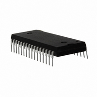
M27C801-100B1 STMicroelectronics, M27C801-100B1 Datasheet - Page 4

M27C801-100B1
Manufacturer Part Number
M27C801-100B1
Description
IC OTP 8MBIT 100NS 32DIP
Manufacturer
STMicroelectronics
Datasheets
1.M27C801-100F1.pdf
(24 pages)
2.M27C801-100B1.pdf
(12 pages)
3.M27C801-100B1.pdf
(16 pages)
Specifications of M27C801-100B1
Format - Memory
EPROMs
Memory Type
OTP EPROM
Memory Size
8M (1M x 8)
Speed
100ns
Interface
Parallel
Voltage - Supply
4.5 V ~ 5.5 V
Operating Temperature
0°C ~ 70°C
Package / Case
32-DIP (0.600", 15.24mm)
Organization
1Mx8
Interface Type
Parallel
In System Programmable
External
Access Time (max)
100ns
Package Type
PDIP
Reprogramming Technique
OTP
Operating Supply Voltage (typ)
5V
Operating Supply Voltage (min)
4.5V
Operating Supply Voltage (max)
5.5V
Supply Current
50mA
Pin Count
32
Mounting
Through Hole
Operating Temp Range
0C to 70C
Operating Temperature Classification
Commercial
Capacitance, Input
6 pF
Capacitance, Output
12 pF
Current, Input, Leakage
±10 μA
Current, Operating
35 mA
Current, Output, Leakage
±10
Current, Supply
35 mA (Max.)
Density
8M
Temperature, Operating
0 to +70 °C
Temperature, Operating, Maximum
70 °C
Temperature, Operating, Minimum
0 °C
Time, Access
100 ns
Time, Fall
≤20 ns
Time, Rise
≤20 ns
Voltage, Input, High
6 V
Voltage, Input, High Level
2 V (Min.)
Voltage, Input, Low
0.8 V
Voltage, Input, Low Level
0.80 V (Max.)
Voltage, Output, High
3.6 V (TTL), 4.3 V (CMOS)
Voltage, Output, Low
0.4 V
Voltage, Supply
5 V
Access Time
45ns
Low Power Consumption
- Active current 35mA at 5 MHz - Standby current 100 μA
Programming Voltage
12.75 V ± 0.25 V
Memory Configuration
1M X 8
Supply Voltage Range
4.5V To 5V
Memory Case Style
DIP
No. Of Pins
32
Rohs Compliant
Yes
Operating Temperature Range
0°C To +70°C
Lead Free Status / RoHS Status
Lead free / RoHS Compliant
Other names
497-1687-5
Available stocks
Company
Part Number
Manufacturer
Quantity
Price
Company:
Part Number:
M27C801-100B1
Manufacturer:
ST
Quantity:
53
Company:
Part Number:
M27C801-100B1
Manufacturer:
ICS
Quantity:
6 107
Part Number:
M27C801-100B1
Manufacturer:
ST
Quantity:
20 000
M27C801
Table 5. AC Measurement Conditions
Figure 3. AC Testing Input Output Waveform
Table 6. Capacitance
Note: 1. Sampled only, not 100% tested.
DEVICE OPERATION
The operating modes of the M27C801 are listed in
the Operating Modes table. A single power supply
is required in the read mode. All inputs are TTL
levels except for GV
tronic Signature and Margin Mode Set or Reset.
Read Mode
The M27C801 has two control functions, both of
which must be logically active in order to obtain
data at the outputs. Chip Enable (E) is the power
control and should be used for device selection.
Output Enable (G) is the output control and should
be used to gate data to the output pins, indepen-
dent of device selection. Assuming that the ad-
4/16
Input Rise and Fall Times
Input Pulse Voltages
Input and Output Timing Ref. Voltages
High Speed
Standard
Symbol
2.4V
0.4V
C
3V
0V
C
OUT
IN
Input Capacitance
Output Capacitance
PP
(1)
Parameter
and 12V on A9 for Elec-
(T
A
= 25 °C, f = 1 MHz)
1.5V
2.0V
0.8V
AI01822
Test Condition
V
V
OUT
High Speed
IN
0 to 3V
= 0V
= 0V
1.5V
Figure 4. AC Testing Load Circuit
dresses are stable, the address access time
(t
(t
of t
E has been low and the addresses have been sta-
ble for at least t
Standby Mode
The M27C801 has a standby mode which reduces
the supply current from 35mA to 100µA.
The M27C801 is placed in the standby mode by
applying a CMOS high signal to the E input. When
in the standby mode, the outputs are in a high im-
pedance state, independent of the GV
10ns
AVQV
ELQV
GLQV
C L = 30pF for High Speed
C L = 100pF for Standard
C L includes JIG capacitance
DEVICE
UNDER
). Data is available at the output after a delay
) is equal to the delay from E to output
TEST
from the falling edge of G, assuming that
AVQV
Min
-t
1.3V
GLQV
20ns (10% to 90%)
1N914
3.3k
.
C L
Max
0.4 to 2.4V
0.8 and 2V
12
Standard
6
PP
OUT
AI01823B
input.
Unit
pF
pF


