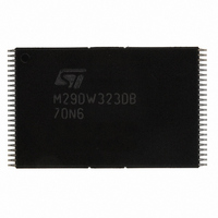
M29DW323DB70N6F NUMONYX, M29DW323DB70N6F Datasheet - Page 49

M29DW323DB70N6F
Manufacturer Part Number
M29DW323DB70N6F
Description
IC FLASH 32MBIT 70NS 48TSOP
Manufacturer
NUMONYX
Series
Axcell™r
Datasheet
1.M29DW323DT70ZE6F.pdf
(51 pages)
Specifications of M29DW323DB70N6F
Format - Memory
FLASH
Memory Type
FLASH - Nor
Memory Size
32M (4Mx8, 2Mx16)
Speed
70ns
Interface
Parallel
Voltage - Supply
2.7 V ~ 3.6 V
Operating Temperature
-40°C ~ 85°C
Package / Case
48-TSOP
Package
48TSOP
Cell Type
NOR
Density
32 Mb
Architecture
Sectored
Block Organization
Asymmetrical
Location Of Boot Block
Bottom
Typical Operating Supply Voltage
3|3.3 V
Sector Size
8KByte x 8|64KByte x 63
Timing Type
Asynchronous
Interface Type
Parallel
Lead Free Status / RoHS Status
Lead free / RoHS Compliant
REVISION HISTORY
Table 33. Document Revision History
07-May-2003
20-Sep-2001
18-Sep-2003
07-Nov-2003
16-Jan-2002
25-Jun-2003
26-Oct-2001
19-Apr-2002
24-Apr-2002
08-Apr-2003
07-Oct-2003
19-Jul-2002
Date
Version
-01
-02
-03
-04
-05
-06
6.1
6.2
7.0
7.1
7.2
7.3
First Issue (Target Specification)
Document expanded to full Product Preview
Corrections made in “Primary Algorithm-Specific Extended Query” Table in Appendix-B
Description of Ready/Busy signal clarified (and
Clarified allowable commands during block erase
Clarified the mode the device returns to in the CFI Read Query command section
tPLYH (time to reset device) re-specified.
Values for addresses 23h and 25h corrected in CFI Query System Interface Information
table in Appendix B
When in Extended Block mode, the block at the boot block address can be used as
OTP. Data Toggle Flow chart corrected. Document promoted from “Product Preview” to
“Preliminary Data”.
Revision numbering modified: a minor revision will be indicated by incrementing the
digit after the dot, and a major revision, by incrementing the digit before the dot
(revision version 06 equals 6.0).
Revision History moved to end of document.
TFBGA48, 6 x 8mm, 0.80mm pitch package added. Identification Current I
from
parameters and notes added to
Endurance
APPENDIX C., EXTENDED MEMORY
read the Extended Memory Block. Extended Memory Block Verify Code row added to
Tables
Address modified in
Status Register
22., Ordering Information
Data, and
View Package
Document promoted from Preliminary Data to full Datasheet status. Packing option
added to
Status of Ready/Busy signal for Erase Suspend Operation modified in
Register
Figures
Table 18., Toggle and Alternative Toggle Bits AC
Note 1 of
Figures
1 and 2 added.
Table 18., Toggle and Alternative Toggle Bits AC Characteristics
Figure 8.
Status of Ready/Busy signal for Program Error, Chip Erase and Block Erase modified in
Table 8., Status Register
Table 20., TSOP48 Lead Plastic Thin Small Outline, 12x20 mm, Package Mechanical
Table 14., DC
3
14
14
and 4,
Bits.
Table 22., Ordering Information
renamed and flowchart modified; Note added.
Table 28., Device Geometry
Figure 18., TSOP48 Lead Plastic Thin Small Outline, 12x20 mm, Bottom
and 15, Toggle and Alternative Toggle Bits Mechanisms modified and Notes
and 15, Toggle and Alternative Toggle Bits Mechanisms added.
Cycles.
Outline, corrected.
Bus Operations, BYTE = VIL
Bits. V
Characteristics. Erase Suspend Latency time and Data Retention
Auto Select
SS
Bits.
pin connection to ground clarified. Note added to
Scheme.
Table 7., Program, Erase Times and Program, Erase
Command. Chip Erase Address modified in
Revision Details
Definition, modified
BLOCK, added.
Scheme.
and
M29DW323DT, M29DW323DB
Figure 16.
Characteristics, added.
Bus Operations, BYTE =
Auto Select Command
modified)
modified.
Table 8., Status
ID
VIH. Bank
Table
Table
removed
sued to
49/51
8.,


