M29DW323DB70N6F NUMONYX, M29DW323DB70N6F Datasheet - Page 4
M29DW323DB70N6F
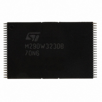
Manufacturer Part Number
M29DW323DB70N6F
Description
IC FLASH 32MBIT 70NS 48TSOP
Manufacturer
NUMONYX
Series
Axcell™r
Datasheet
1.M29DW323DT70ZE6F.pdf
(51 pages)
Specifications of M29DW323DB70N6F
Format - Memory
FLASH
Memory Type
FLASH - Nor
Memory Size
32M (4Mx8, 2Mx16)
Speed
70ns
Interface
Parallel
Voltage - Supply
2.7 V ~ 3.6 V
Operating Temperature
-40°C ~ 85°C
Package / Case
48-TSOP
Package
48TSOP
Cell Type
NOR
Density
32 Mb
Architecture
Sectored
Block Organization
Asymmetrical
Location Of Boot Block
Bottom
Typical Operating Supply Voltage
3|3.3 V
Sector Size
8KByte x 8|64KByte x 63
Timing Type
Asynchronous
Interface Type
Parallel
Lead Free Status / RoHS Status
Lead free / RoHS Compliant


M29DW323DT, M29DW323DB
PACKAGE MECHANICAL . . . . . . . . . . . . . . . . . . . . . . . . . . . . . . . . . . . . . . . . . . . . . . . . . . . . . . . . . . 31
PART NUMBERING . . . . . . . . . . . . . . . . . . . . . . . . . . . . . . . . . . . . . . . . . . . . . . . . . . . . . . . . . . . . . . . 33
APPENDIX A.BLOCK ADDRESSES . . . . . . . . . . . . . . . . . . . . . . . . . . . . . . . . . . . . . . . . . . . . . . . . . . 34
APPENDIX B.COMMON FLASH INTERFACE (CFI) . . . . . . . . . . . . . . . . . . . . . . . . . . . . . . . . . . . . . . 40
APPENDIX C.EXTENDED MEMORY BLOCK . . . . . . . . . . . . . . . . . . . . . . . . . . . . . . . . . . . . . . . . . . . 43
APPENDIX D.BLOCK PROTECTION. . . . . . . . . . . . . . . . . . . . . . . . . . . . . . . . . . . . . . . . . . . . . . . . . . 44
REVISION HISTORY. . . . . . . . . . . . . . . . . . . . . . . . . . . . . . . . . . . . . . . . . . . . . . . . . . . . . . . . . . . . . . . 49
4/51
Figure 13.Write AC Waveforms, Chip Enable Controlled . . . . . . . . . . . . . . . . . . . . . . . . . . . . . . . . 28
Table 17. Write AC Characteristics, Chip Enable Controlled. . . . . . . . . . . . . . . . . . . . . . . . . . . . . . 28
Figure 14.Toggle and Alternative Toggle Bits Mechanism, Chip Enable Controlled . . . . . . . . . . . . 29
Figure 15.Toggle and Alternative Toggle Bits Mechanism, Output Enable Controlled . . . . . . . . . . 29
Table 18. Toggle and Alternative Toggle Bits AC Characteristics . . . . . . . . . . . . . . . . . . . . . . . . . . 29
Figure 16.Reset/Block Temporary Unprotect AC Waveforms . . . . . . . . . . . . . . . . . . . . . . . . . . . . . 30
Table 19. Reset/Block Temporary Unprotect AC Characteristics . . . . . . . . . . . . . . . . . . . . . . . . . . 30
Figure 17.Accelerated Program Timing Waveforms . . . . . . . . . . . . . . . . . . . . . . . . . . . . . . . . . . . . 30
Figure 18.TSOP48 Lead Plastic Thin Small Outline, 12x20 mm, Bottom View Package Outline . . 31
Table 20. TSOP48 Lead Plastic Thin Small Outline, 12x20 mm, Package Mechanical Data . . . . . 31
Figure 19.TFBGA48 6x8mm - 6x8 Ball Array, 0.8mm Pitch, Bottom View Package Outline. . . . . . 32
Table 21. TFBGA48 6x8mm - 6x8 Ball Array, 0.8mm Pitch, Package Mechanical Data. . . . . . . . . 32
Table 22. Ordering Information Scheme . . . . . . . . . . . . . . . . . . . . . . . . . . . . . . . . . . . . . . . . . . . . . 33
Table 23. Top Boot Block Addresses, M29DW323DT. . . . . . . . . . . . . . . . . . . . . . . . . . . . . . . . . . . 34
Table 24. Bottom Boot Block Addresses, M29DW323DB . . . . . . . . . . . . . . . . . . . . . . . . . . . . . . . . 37
Table 25. Query Structure Overview . . . . . . . . . . . . . . . . . . . . . . . . . . . . . . . . . . . . . . . . . . . . . . . . 40
Table 26. CFI Query Identification String. . . . . . . . . . . . . . . . . . . . . . . . . . . . . . . . . . . . . . . . . . . . . 40
Table 27. CFI Query System Interface Information . . . . . . . . . . . . . . . . . . . . . . . . . . . . . . . . . . . . . 41
Table 28. Device Geometry Definition . . . . . . . . . . . . . . . . . . . . . . . . . . . . . . . . . . . . . . . . . . . . . . 41
Table 29. Primary Algorithm-Specific Extended Query Table . . . . . . . . . . . . . . . . . . . . . . . . . . . . . 42
Table 30. Security Code Area . . . . . . . . . . . . . . . . . . . . . . . . . . . . . . . . . . . . . . . . . . . . . . . . . . . . . 42
Factory Locked Extended Block . . . . . . . . . . . . . . . . . . . . . . . . . . . . . . . . . . . . . . . . . . . . . . . . . 43
Customer Lockable Extended Block . . . . . . . . . . . . . . . . . . . . . . . . . . . . . . . . . . . . . . . . . . . . . . 43
Table 31. Extended Block Address and Data . . . . . . . . . . . . . . . . . . . . . . . . . . . . . . . . . . . . . . . . . 43
Programmer Technique . . . . . . . . . . . . . . . . . . . . . . . . . . . . . . . . . . . . . . . . . . . . . . . . . . . . . . . . 44
In-System Technique . . . . . . . . . . . . . . . . . . . . . . . . . . . . . . . . . . . . . . . . . . . . . . . . . . . . . . . . . . 44
Table 32. Programmer Technique Bus Operations, BYTE = V
Figure 20.Programmer Equipment Group Protect Flowchart . . . . . . . . . . . . . . . . . . . . . . . . . . . . . 45
Figure 21.Programmer Equipment Chip Unprotect Flowchart. . . . . . . . . . . . . . . . . . . . . . . . . . . . . 46
Figure 22.In-System Equipment Group Protect Flowchart . . . . . . . . . . . . . . . . . . . . . . . . . . . . . . . 47
Figure 23.In-System Equipment Chip Unprotect Flowchart . . . . . . . . . . . . . . . . . . . . . . . . . . . . . . 48
IH
or V
IL . . . . . . . . . . . . . . . . . . . . . . . . . . . 44
Related parts for M29DW323DB70N6F
Image
Part Number
Description
Manufacturer
Datasheet
Request
R

Part Number:
Description:
32 Mbit 4mb X8 Or 2mb X16, Dual Bank 8 24, Boot Block 3v Supply Flash Memory
Manufacturer:
Numonyx
Datasheet:
Part Number:
Description:
Numonyx� Embedded Flash Memory J3 V. D
Manufacturer:
Numonyx
Datasheet:
Part Number:
Description:
Manufacturer:
NUMONYX
Datasheet:
Part Number:
Description:
Manufacturer:
NUMONYX
Datasheet: