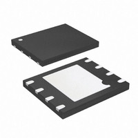
AT25DF161-MH-Y Atmel, AT25DF161-MH-Y Datasheet - Page 27

AT25DF161-MH-Y
Manufacturer Part Number
AT25DF161-MH-Y
Description
IC FLASH 16MBIT 100MHZ 8UDFN
Manufacturer
Atmel
Datasheet
1.AT25DF161-SH-B.pdf
(52 pages)
Specifications of AT25DF161-MH-Y
Format - Memory
FLASH
Memory Type
DataFLASH
Memory Size
16M (2M x 8)
Speed
100MHz
Interface
SPI, RapidS
Voltage - Supply
2.7 V ~ 3.6 V
Operating Temperature
-40°C ~ 85°C
Package / Case
8-UDFN
Lead Free Status / RoHS Status
Lead free / RoHS Compliant
Available stocks
Company
Part Number
Manufacturer
Quantity
Price
Part Number:
AT25DF161-MH-Y
Manufacturer:
ATMEL/爱特梅尔
Quantity:
20 000
3687E–DFLASH–11/10
10.3
10.4
Read Sector Lockdown Registers
The Sector Lockdown Registers can be read to determine the current lockdown status of each physical 64-Kbyte sector.
To read the Sector Lockdown Register for a particular 64-Kbyte sector, the CS pin must first be asserted and the opcode of
35h must be clocked in. Once the opcode has been clocked in, three address bytes designating any address within the 64-
Kbyte sector must be clocked in. After the address bytes have been clocked in, data will be output on the SO pin during
every subsequent clock cycle. The data being output will be a repeating byte of either FFh or 00h to denote the value of
the appropriate Sector Lockdown Register.
At clock frequencies above f
above f
appropriate Sector Lockdown Register.
Table 10-2.
Deasserting the CS pin will terminate the read operation and put the SO pin into a high-impedance state. The CS pin can
be deasserted at any time and does not require that a full byte of data be read.
Figure 10-3. Read Sector Lockdown Register
Program OTP Security Register
The device contains a specialized OTP (One-Time Programmable) Security Register that can be used for purposes such as
unique device serialization, system-level Electronic Serial Number (ESN) storage, locked key storage, etc. The OTP
Security Register is independent of the main Flash memory array and is comprised of a total of 128-bytes of memory
divided into two portions. The first 64-bytes (byte locations 0 through 63) of the OTP Security Register are allocated as a
one-time user-programmable space. Once these 64-bytes have been programmed, they cannot be erased or
reprogrammed. The remaining 64-bytes of the OTP Security Register (byte locations 64 through 127) are factory
programmed by Atmel
be changed.
Output Data
SCK
SO
CS
SI
00h
FFh
CLK
, at least two bytes of data must be clocked out from the device in order to determine the correct status of the
Read Sector Lockdown Register – Output Data
Sector Lockdown Register Value
Sector Lockdown Register value is 0 (sector is not locked down)
Sector Lockdown Register value is 1 (sector is permanently locked down).
®
and will contain a unique value for each device. The factory programmed data is fixed and cannot
CLK
, the first byte of data output will not be valid. Therefore, if operating at clock frequencies
Atmel AT25DF161
27


