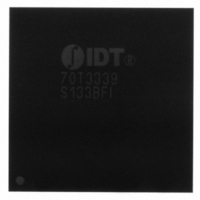
IDT70T3339S133BFI IDT, Integrated Device Technology Inc, IDT70T3339S133BFI Datasheet - Page 5

IDT70T3339S133BFI
Manufacturer Part Number
IDT70T3339S133BFI
Description
IC SRAM 9MBIT 133MHZ 208FBGA
Manufacturer
IDT, Integrated Device Technology Inc
Datasheet
1.IDT70T3339S133BFI.pdf
(27 pages)
Specifications of IDT70T3339S133BFI
Format - Memory
RAM
Memory Type
SRAM - Dual Port, Synchronous
Memory Size
9M (512K x 18)
Speed
133MHz
Interface
Parallel
Voltage - Supply
2.4 V ~ 2.6 V
Operating Temperature
-40°C ~ 85°C
Package / Case
208-FBGA
Lead Free Status / RoHS Status
Lead free / RoHS Compliant
Other names
70T3339S133BFI
800-1378
800-1378
Available stocks
Company
Part Number
Manufacturer
Quantity
Price
Company:
Part Number:
IDT70T3339S133BFI
Manufacturer:
IDT
Quantity:
850
Company:
Part Number:
IDT70T3339S133BFI
Manufacturer:
IDT, Integrated Device Technology Inc
Quantity:
10 000
Company:
Part Number:
IDT70T3339S133BFI8
Manufacturer:
IDT, Integrated Device Technology Inc
Quantity:
10 000
Pin Names
CE
R/W
OE
A
I/O
CLK
PL/FT
ADS
CNTEN
REPEAT
UB
LB
IDT70T3339/19/99S
High-Speed 2.5V 512/256/128K x 18 Dual-Port Static RAM
0L
0L
0L
L
L
L
L
- A
L
,
L
Left Port
- I/O
CE
L
COL
V
18L
OPT
INT
L
ZZ
DDQL
1L
L
(5)
17L
L
L
L
L
TRST
TMS
TCK
V
V
TDI
TDI
DD
SS
R/W
I/O
CLK
PL/FT
CE
OE
A
ADS
CNTEN
REPEAT
UB
LB
0R
0R
R
0R
R
R
R
R
- A
Right Port
R
,
- I/O
R
CE
COL
V
INT
OPT
18R
R
DDQR
ZZ
R
1R
17R
(5)
R
R
R
R
Chip Enables (Input)
Read/Write Enable (Input)
Output Enable (Input)
Data Input/Output
Clock (Input)
Pipeline/Flow-Through (Input)
Counter Enable (Input)
Counter Repeat
Upper Byte Enable (I/O
Lower Byte Enable (I/O
Power (I/O Bus) (3.3V or 2.5V)
Option for selecting V
Sleep Mode pin
Power (2.5V)
Ground (0V) (Input)
Reset (Initialize TAP Controller) (Input)
Interrupt Flag (Output)
Collision Alert (Output)
Address (Input)
Address Strobe Enable (Input)
Test Data Input
Test Data Output
Test Logic Clock (10MHz) (Input)
Test Mode Select (Input)
(1)
(Input)
(3)
Names
(4)
(Input)
(6)
DDQX
0
9
- I/O
- I/O
(1,2)
8
17
(Input)
)
(6)
(1)
)
(6)
5652 tbl 01
(Input)
6.42
5
NOTES:
1. V
2. OPT
3. When REPEAT
4. The sleep mode pin shuts off all dynamic inputs, except JTAG inputs, when
5. Address A
6. Chip Enables and Byte Enables are double buffered when PL/FT = V
applying inputs on the I/Os and controls for that port.
If OPT
levels and V
port's I/Os and address controls will operate at 2.5V levels and V
supplied at 2.5V. The OPT pins are independent of one another—both ports can
operate at 3.3V levels, both can operate at 2.5V levels, or either can operate
at 3.3V with the other at 2.5V.
via ADS
asserted. All static inputs, i.e., PL/FTx and OPTx and the sleep mode pins
themselves (ZZx) are not affected during sleep mode. It is recommended that
boundry scan not be operated during sleep mode.
NC's for the IDT70T3399.
signals take two cycles to deselect.
DD
, OPT
X
selects the operating voltage levels for the I/Os and controls on that port.
X
is set to V
X
.
X
18x
, and V
DDQX
is a NC for the IDT70T3319. Also, Addresses A
X
is asserted, the counter will reset to the last valid address loaded
Industrial and Commercial Temperature Ranges
DD
must be supplied at 3.3V. If OPT
DDQX
(2.5V), then that port's I/Os and controls will operate at 3.3V
must be set to appropriate operating levels prior to
X
is set to V
SS
18x
(0V), then that
DDQX
and A
IH
, i.e., the
must be
17x
are


