CY62158EV30LL-45ZSXI Cypress Semiconductor Corp, CY62158EV30LL-45ZSXI Datasheet
CY62158EV30LL-45ZSXI
Specifications of CY62158EV30LL-45ZSXI
CY62158EV30LL-45ZSXI
Available stocks


Related parts for CY62158EV30LL-45ZSXI

CY62158EV30LL-45ZSXI Summary of contents
Page 1
... Offered in Pb-free 48-ball VFBGA and 44-pin TSOP II ■ packages Logic Block Diagram Cypress Semiconductor Corporation Document #: 38-05578 Rev. *G 8-Mbit (1024 K × 8) Static RAM Functional Description The CY62158EV30 is a high performance CMOS static RAM organized as 1024K words by 8 bits. This device features advanced circuit design to provide ultra low active current. This is ideal for providing More Battery Life™ ...
Page 2
Contents Pin Configurations ...........................................................3 Product Portfolio ..............................................................3 Maximum Ratings .............................................................4 Operating Range ...............................................................4 Electrical Characteristics .................................................4 Capacitance ......................................................................5 Thermal Resistance ..........................................................5 AC Test Loads and Waveforms .......................................5 Data Retention Characteristics .......................................6 Data Retention Waveform ................................................6 Switching Characteristics ................................................7 Switching Waveforms ...
Page 3
... Product Portfolio V Range (V) CC Product [2] Min Typ CY62158EV30LL 2.2 3.0 Notes 1. NC pins are not connected on the die. 2. Typical values are included for reference only and are not guaranteed or tested. Typical values are measured at V Document #: 38-05578 Rev I I I/O ...
Page 4
... CMOS level to meet the Document #: 38-05578 Rev Input Voltage Output Current into Outputs (LOW) ............................20 mA Static Discharge Voltage ........................................> 2001 V (MIL-STD-883, Method 3015) Latch up Current ....................................................> 200 mA Operating Range + 0.3 V Product CC(max) + 0.3 V CY62158EV30LL CC(max) Test Conditions I = –0 –1.0 mA, V > 2.1 mA, V > ...
Page 5
Capacitance [8] Parameter Description C Input Capacitance IN C Output Capacitance OUT Thermal Resistance [8] Parameter Description Thermal Resistance JA (Junction to Ambient) Thermal Resistance JC (Junction to Case) AC Test Loads and Waveforms OUTPUT ...
Page 6
Data Retention Characteristics Over the Operating Range Parameter Description V V for Data Retention DR CC [10] I Data Retention Current CCDR [11] t Chip Deselect to Data Retention Time CDR [12] t Operation Recovery Time R Data Retention Waveform ...
Page 7
... HZOE HZCE HZWE 16. The internal write time of the memory is defined by the overlap of WE, CE signals can terminate a write by going INACTIVE. The data input setup and hold timing should be referenced to the edge of the signal that terminates the write. Document #: 38-05578 Rev. *G Description ...
Page 8
Switching Waveforms Read Cycle No. 1 (Address Transition Controlled) ADDRESS PREVIOUS DATA VALID DATA OUT [18, 19] Read Cycle No. 2 (OE Controlled) ADDRESS ACE OE t LZOE HIGH IMPEDANCE DATA OUT t LZCE V ...
Page 9
... WE OE DATA I/O Notes 20. The internal write time of the memory is defined by the overlap of WE, CE signals can terminate a write by going INACTIVE. The data input setup and hold timing should be referenced to the edge of the signal that terminates the write. 21. Data I/O is high impedance ...
Page 10
Switching Waveforms (continued) Write Cycle No. 3 (WE Controlled, OE LOW) ADDRESS DATA I/O NOTE 25 t HZWE Truth Table [26 [26] X ...
Page 11
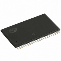
... Ordering Information Speed Ordering Code (ns) 45 CY62158EV30LL-45BVXI CY62158EV30LL-45ZSXI Contact your local Cypress sales representative for availability of these parts. Ordering Code Definitions E V30 LL 621 Document #: 38-05578 Rev. *G Package Package Type Diagram 51-85150 48-ball Very Fine-Pitch Ball Grid Array (Pb-free) 51-85087 44-pin Thin Small Outline Package Type II (Pb-free) ...
Page 12
Package Diagrams Figure 1. 48-ball VFBGA (6 × 8 × 1 mm) BV48/BZ48, 51-85150 Document #: 38-05578 Rev. *G ® CY62158EV30 MoBL 51-85150 *F Page [+] Feedback ...
Page 13
Package Diagrams (continued) Document #: 38-05578 Rev. *G Figure 2. 44-pin TSOP Z44-II, 51-85087 ® CY62158EV30 MoBL 51-85087 *C Page [+] Feedback ...
Page 14
... CMOS complementary metal oxide semiconductor I/O input/output OE output enable RAM random access memory SRAM static random access memory TTL transistor-transistor logic TSOP thin small outline package VFBGA very fine-pitch ball grid array WE write enable Document #: 38-05578 Rev. *G CY62158EV30 MoBL ...
Page 15
Document History Page ® Document Title: CY62158EV30 MoBL Document Number: 38-05578 Orig. of Rev. ECN No. Issue Date Change ** 270329 See ECN *A 291271 See ECN *B 444306 See ECN NXR *C 467052 See ECN NXR *D 1015643 See ...
Page 16
... Cypress against all charges. Any Source Code (software and/or firmware) is owned by Cypress Semiconductor Corporation (Cypress) and is protected by and subject to worldwide patent protection (United States and foreign), United States copyright laws and international treaty provisions. Cypress hereby grants to licensee a personal, non-exclusive, non-transferable license to copy, use, modify, create derivative works of, and compile the Cypress Source Code and derivative works for the sole purpose of creating custom software and or firmware in support of licensee product to be used only in conjunction with a Cypress integrated circuit as specified in the applicable agreement ...