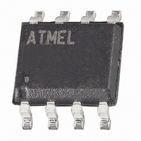
AT93C56A-10SU-2.7 Atmel, AT93C56A-10SU-2.7 Datasheet - Page 7

AT93C56A-10SU-2.7
Manufacturer Part Number
AT93C56A-10SU-2.7
Description
IC EEPROM 2KBIT 2MHZ 8SOIC
Manufacturer
Atmel
Specifications of AT93C56A-10SU-2.7
Format - Memory
EEPROMs - Serial
Memory Type
EEPROM
Memory Size
2K (256 x 8 or 128 x 16)
Speed
1MHz, 2MHz
Interface
3-Wire Serial
Voltage - Supply
2.7 V ~ 5.5 V
Operating Temperature
-40°C ~ 85°C
Package / Case
8-SOIC (3.9mm Width)
Organization
256 x 8 or 128 K x 16
Interface Type
3-Wire
Maximum Clock Frequency
1 MHz
Supply Voltage (max)
5.5 V
Supply Voltage (min)
2.7 V
Maximum Operating Current
2 mA
Maximum Operating Temperature
+ 85 C
Mounting Style
SMD/SMT
Minimum Operating Temperature
- 40 C
Operating Supply Voltage
3.3 V, 5 V
Capacitance, Input
5 pF
Capacitance, Output
5 pF
Current, Input, Leakage
0.1 μA
Current, Operating
0.5 mA
Current, Output, Leakage
0.1
Data Retention
100 yrs.
Density
2K
Package Type
JEDEC SOIC
Temperature, Operating
-40 to +85 °C
Time, Address Setup
50
Time, Fall
250 ns
Time, Rise
250 ns
Voltage, Input, High
3.7 to 6.5 V
Voltage, Input, Low
0.8 V
Voltage, Output, High
2.4 V
Voltage, Output, Low
0.4 V
Voltage, Supply
2.7 to 5.5 V
Lead Free Status / RoHS Status
Lead free / RoHS Compliant
Available stocks
Company
Part Number
Manufacturer
Quantity
Price
Part Number:
AT93C56A-10SU-2.7
Manufacturer:
ATMEL/爱特梅尔
Quantity:
20 000
4. Functional Description
3378O–SEEPR–11/09
The AT93C56A/66A is accessed via a simple and versatile three-wire serial communication
interface. Device operation is controlled by seven instructions issued by the host processor. A
valid instruction starts with a rising edge of CS and consists of a Start Bit (logic “1”) followed
by the appropriate Op Code and the desired memory address location.
READ (READ): The Read (READ) instruction contains the address code for the memory loca-
tion to be read. After the instruction and address are decoded, data from the selected memory
location is available at the serial output pin DO. Output data changes are synchronized with the
rising edges of serial clock SK. It should be noted that a dummy bit (logic “0”) precedes the 8- or
16-bit data output string. The AT93C56A/66A supports sequential read operations. The device
will automatically increment the internal address pointer and clock out the next memory location
as long as Chip Select (CS) is held high. In this case, the dummy bit (logic “0”) will not be
clocked out between memory locations, thus allowing for a continuous stream of data to be read.
ERASE/WRITE (EWEN): To assure data integrity, the part automatically goes into the
Erase/Write Disable (EWDS) state when power is first applied. An Erase/Write Enable (EWEN)
instruction must be executed first before any programming instructions can be carried out.
Please note that once in the EWEN state, programming remains enabled until an EWDS instruc-
tion is executed or V
ERASE (ERASE): The Erase instruction programs all bits in the specified memory location to
the logical “1” state. The self-timed erase cycle starts once the ERASE instruction and address
are decoded. The DO pin outputs the Ready/Busy status of the part if CS is brought high after
being kept low for a minimum of 250 ns (t
memory location has been erased, and the part is ready for another instruction.
WRITE (WRITE): The Write (WRITE) instruction contains the 8 or 16 bits of data to be written
into the specified memory location. The self-timed programming cycle t
of data is received at serial data input pin DI. The DO pin outputs the Ready/Busy status of the
part if CS is brought high after being kept low for a minimum of 250 ns (t
indicates that programming is still in progress. A logic “1” indicates that the memory location at
the specified address has been written with the data pattern contained in the instruction and the
part is ready for further instructions. A READY/BUSY status cannot be obtained if the CS is
brought high after the end of the self-timed programming cycle t
ERASE ALL (ERAL): The Erase All (ERAL) instruction programs every bit in the memory array
to the logic “1” state and is primarily used for testing purposes. The DO pin outputs the
Ready/Busy status of the part if CS is brought high after being kept low for a minimum of 250 ns
(t
WRITE ALL (WRAL): The Write All (WRAL) instruction programs all memory locations with the
data patterns specified in the instruction. The DO pin outputs the Ready/Busy status of the part if
CS is brought high after being kept low for a minimum of 250 ns (t
valid only at V
ERASE/WRITE DISABLE (EWDS): To protect against accidental data disturb, the Erase/Write
Disable (EWDS) instruction disables all programming modes and should be executed after all
programming operations. The operation of the READ instruction is independent of both the
EWEN and EWDS instructions and can be executed at any time.
CS
). The ERAL instruction is valid only at V
CC
= 5.0V ± 10%.
CC
power is removed from the part.
CS
CC
). A logic “1” at pin DO indicates that the selected
= 5.0V ± 10%.
CS
AT93C56A/66A
WP
). The WRAL instruction is
WP
.
starts after the last bit
CS
). A logic “0” at DO
7


