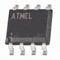
AT93C56A-10SU-2.7 Atmel, AT93C56A-10SU-2.7 Datasheet - Page 16

AT93C56A-10SU-2.7
Manufacturer Part Number
AT93C56A-10SU-2.7
Description
IC EEPROM 2KBIT 2MHZ 8SOIC
Manufacturer
Atmel
Specifications of AT93C56A-10SU-2.7
Format - Memory
EEPROMs - Serial
Memory Type
EEPROM
Memory Size
2K (256 x 8 or 128 x 16)
Speed
1MHz, 2MHz
Interface
3-Wire Serial
Voltage - Supply
2.7 V ~ 5.5 V
Operating Temperature
-40°C ~ 85°C
Package / Case
8-SOIC (3.9mm Width)
Organization
256 x 8 or 128 K x 16
Interface Type
3-Wire
Maximum Clock Frequency
1 MHz
Supply Voltage (max)
5.5 V
Supply Voltage (min)
2.7 V
Maximum Operating Current
2 mA
Maximum Operating Temperature
+ 85 C
Mounting Style
SMD/SMT
Minimum Operating Temperature
- 40 C
Operating Supply Voltage
3.3 V, 5 V
Capacitance, Input
5 pF
Capacitance, Output
5 pF
Current, Input, Leakage
0.1 μA
Current, Operating
0.5 mA
Current, Output, Leakage
0.1
Data Retention
100 yrs.
Density
2K
Package Type
JEDEC SOIC
Temperature, Operating
-40 to +85 °C
Time, Address Setup
50
Time, Fall
250 ns
Time, Rise
250 ns
Voltage, Input, High
3.7 to 6.5 V
Voltage, Input, Low
0.8 V
Voltage, Output, High
2.4 V
Voltage, Output, Low
0.4 V
Voltage, Supply
2.7 to 5.5 V
Lead Free Status / RoHS Status
Lead free / RoHS Compliant
Available stocks
Company
Part Number
Manufacturer
Quantity
Price
Part Number:
AT93C56A-10SU-2.7
Manufacturer:
ATMEL/爱特梅尔
Quantity:
20 000
8.3
16
Notes: 1. This drawing is for general information only; refer to EIAJ Drawing EDR-7320 for additional information.
Notes: 1. This drawing is for general information only; refer to EIAJ Drawing EDR-7320 for additional information.
8S2 – EIAJ SOIC
2. Mismatch of the upper and lower dies and resin burrs aren't included.
3. It is recommended that upper and lower cavities be equal. If they are different, the larger dimension shall be regarded.
4. Determines the true geometric position.
5. Values b,C apply to plated terminal. The standard thickness of the plating layer shall measure between 0.007 to .021 mm.
2. Mismatch of the upper and lower dies and resin burrs are not included.
3. It is recommended that upper and lower cavities be equal. If they are different, the larger dimension shall be regarded.
4. Determines the true geometric position.
5. Values b and C apply to pb/Sn solder plated terminal. The standard thickness of the solder layer shall be 0.010 +0.010/−0.005 mm.
AT93C56A/66A
R
R
2325 Orchard Parkway
San Jose, CA 95131
e
2325 Orchard Parkway
San Jose, CA 95131
e
Top View
Side View
SIDE VIEW
TOP VIEW
D
D
1
N
N
1 1
A
b
TITLE
TITLE
8S2, 8-lead, 0.209" Body, Plastic Small
Outline Package (EIAJ)
8S2, 8-lead, 0.209" Body, Plastic Small
Outline Package (EIAJ)
A
b
A1
E
A1
E
C
End View
∅
SYMBOL
A
A1
b
C
D
E1
E
L
θ
e
SYMBOL
L
E1
END VIEW
A
A1
b
C
D
E1
E
L
∅
e
1.70
0.05
0.35
0.15
5.13
5.18
7.70
0.51
0˚
MIN
θ θ
COMMON DIMENSIONS
(Unit of Measure = mm)
COMMON DIMENSIONS
1.70
0.05
0.35
0.15
5.13
5.18
7.70
0.51
MIN
1.27 BSC
(Unit of Measure = mm)
0˚
NOM
L
E1
E
1.27 BSC
NOM
DRAWING NO.
MAX
2.16
0.25
0.48
0.35
5.35
5.40
8.26
0.85
8˚
DRAWING NO.
8S2
MAX
2.16
0.25
0.48
0.35
5.35
5.40
8.26
0.85
8˚
8S2
3378O–SEEPR–11/09
NOTE
5
5
2, 3
4
04/07/06
NOTE
5
5
2, 3
4
REV.
10/7/03
D
REV.
C


