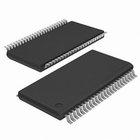
IDT74SSTVF16857PAG IDT, Integrated Device Technology Inc, IDT74SSTVF16857PAG Datasheet - Page 2

IDT74SSTVF16857PAG
Manufacturer Part Number
IDT74SSTVF16857PAG
Description
IC BUFFER 14BIT SSTL I/O 48-TSSO
Manufacturer
IDT, Integrated Device Technology Inc
Series
74SSTVFr
Datasheet
1.IDT74SSTVF16857PAG8.pdf
(6 pages)
Specifications of IDT74SSTVF16857PAG
Logic Type
Registered Buffer with SSTL_2 Inputs and Outputs
Supply Voltage
2.3 V ~ 2.7 V
Number Of Bits
14
Operating Temperature
-40°C ~ 85°C
Mounting Type
Surface Mount
Package / Case
48-TSSOP
Lead Free Status / RoHS Status
Lead free / RoHS Compliant
Other names
74SSTVF16857PAG
Available stocks
Company
Part Number
Manufacturer
Quantity
Price
Part Number:
IDT74SSTVF16857PAG
Manufacturer:
IDT
Quantity:
20 000
PIN CONFIGURATION
IDT74SSTVF16857
14-BIT REGISTERED BUFFER WITH SSTL I/O
V
V
V
V
V
GND
GND
GND
GND
GND
DDQ
Q
Q
DDQ
Q
DDQ
DDQ
DDQ
Q
Q
Q
Q
Q
Q
Q
Q
Q
Q
Q
11
12
13
10
14
1
3
4
5
6
7
8
9
2
10
11
12
13
14
15
16
17
18
19
1
20
21
22
23
24
2
3
4
5
6
7
8
9
TOP VIEW
TSSOP
42
41
48
47
46
45
44
43
40
39
38
37
36
35
34
33
32
31
30
29
28
27
26
25
D
D
GND
V
D
D
D
D
D
CLK
CLK
V
GND
V
RESET
D
D
D
D
D
V
GND
D
D
1
2
DD
3
4
5
6
7
DD
REF
8
9
10
11
12
DD
13
14
2
NOTES:
1. Stresses greater than those listed under ABSOLUTE MAXIMUM RATINGS may cause
2. The input and output negative voltage ratings may be exceeded if the ratings of the
3. The output current will flow if the following conditions are observed:
FUNCTION TABLE
NOTES:
1. H = HIGH Voltage Level
2. Qo = Output level before the indicated steady-state conditions were established.
ABSOLUTE MAXIMUM RATINGS
V
L = LOW Voltage Level
X = Don’t Care
↑ = LOW to HIGH
↓ = HIGH to LOW
DD
a) Output in HIGH state
b) V
Symbol
permanent damage to the device. This is a stress rating only and functional operation
of the device at these or any other conditions above those indicated in the operational
sections of this specification is not implied. Exposure to absolute maximum rating
conditions for extended periods may affect reliability.
I/P and O/P clamp current are observed.
RESET
V
T
V
V
or V
I
I
OK
I
STG
O
I
IK
DD
O
(2)
H
H
H
(3)
L
O
DDQ
= V
DDQ
Description
Supply Voltage Range
Input Voltage Range
Output Voltage Range
Input Clamp Current, V
Output Clamp Current,
V
Continuous Output Current,
V
Continuous Current through each
V
Storage Temperature Range
O
O
DD
= 0 to V
< 0 or V
L or H
, V
CLK
↑
↑
X
DDQ
Input
DDQ
or GND
O
> V
COMMERCIAL TEMPERATURE RANGE
DDQ
L or H
CLK
↓
↓
X
I
(1)
< 0
–0.5 to V
–0.5 to V
D
H
L
X
X
–65 to +150
–0.5 to 3.6
Max.
±100
±50
±50
–50
DDQ
DD
+0.5
+0.5
Q Outputs
(1)
Qo
H
L
L
(2)
Unit
mA
mA
mA
mA
°C
V
V
V


