CD4015BCN Fairchild Semiconductor, CD4015BCN Datasheet
CD4015BCN
Specifications of CD4015BCN
4015B
CD4015
CD4015CN
Available stocks


Related parts for CD4015BCN


CD4015BCN Summary of contents
Page 1
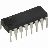
... Ordering Code: Order Number Package Number CD4015BCM M16A 16-Lead Small Outline Integrated Circuit (SOIC), JEDEC MS-012, 0.150" Narrow CD4015BCN N16E 16-Lead Plastic Dual-In-Line Package (PDIP), JEDEC MS-001, 0.300" Wide Connection Diagram © 2004 Fairchild Semiconductor Corporation Features Wide supply voltage range: High noise immunity: 0 ...
Page 2
Logic Diagrams Terminal No Terminal No. 8 GND www.fairchildsemi.com 2 ...
Page 3
Absolute Maximum Ratings (Note 3) DC Supply Voltage ( Input Voltage ( Storage Temperature Range ( Power Dissipation ( Dual-In-Line Small Outline Lead Temperature ( (Soldering, 10 ...
Page 4
AC Electrical Characteristics pF, R 200k ns, unless otherwise specified Symbol Parameter CLOCK OPERATION Propagation Delay Time PHL PLH Transition Time ...
Page 5
Physical Dimensions inches (millimeters) unless otherwise noted 16-Lead Small Outline Integrated Circuit (SOIC), JEDEC MS-012, 0.150" Narrow Package Number M16A 5 www.fairchildsemi.com ...
Page 6
Physical Dimensions inches (millimeters) unless otherwise noted (Continued) 16-Lead Plastic Dual-In-Line Package (PDIP), JEDEC MS-001, 0.300" Wide Fairchild does not assume any responsibility for use of any circuitry described, no circuit patent licenses are implied and Fairchild reserves the right ...