MM74HC589M Fairchild Semiconductor, MM74HC589M Datasheet
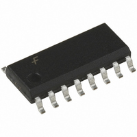
IC SHIFT REGISTER 8-BIT 16-SOIC

MM74HC589M

Manufacturer Part Number
MM74HC589M
Description
IC SHIFT REGISTER 8-BIT 16-SOIC
Manufacturer
Fairchild Semiconductor
Series
74HCr
Datasheet

Specifications of MM74HC589M

Logic Type
Shift Register
Output Type
Standard
Number Of Elements
1
Number Of Bits Per Element
8
Function
Universal
Voltage - Supply
2 V ~ 6 V
Operating Temperature
-40°C ~ 85°C
Mounting Type
Surface Mount
Package / Case
16-SOIC (3.9mm Width)
Counting Sequence
Serial/Parallel to Serial
Number Of Circuits
1
Logic Family
74HC
Propagation Delay Time
210 ns, 42 ns, 36 ns
Supply Voltage (max)
6 V
Maximum Operating Temperature
+ 85 C
Minimum Operating Temperature
- 40 C
Mounting Style
SMD/SMT
Operating Supply Voltage
2 V to 6 V
Lead Free Status / RoHS Status
Lead free / RoHS Compliant

Available stocks

Company
Part Number
Manufacturer
Quantity
Price
Part Number:
MM74HC589M
Manufacturer:
FAIRCHILD/仙童
Quantity:
20 000
© 2001 Fairchild Semiconductor Corporation
MM74HC589M
MM74HC589SJ
MM74HC589N
MM74HC589
8-Bit Shift Registers
with Input Latches and 3-STATE Serial Output
General Description
The MM74HC589 high speed shift register utilizes
advanced silicon-gate CMOS technology to achieve the
high noise immunity and low power consumption of stan-
dard CMOS integrated circuits, as well as the ability to
drive 15 LS-TTL loads.
The MM74HC589 comes in a 16-pin package and consists
of an 8-bit storage latch feeding a parallel-in, serial-out 8-
bit shift register. Data can also be entered serially the shift
register through the SER pin. Both the storage register and
shift register have positive-edge triggered clocks, RCK and
SCK, respectively. SLOAD pin controls parallel LOAD or
serial shift operations for the shift register. The shift register
has a 3-STATE output to enable the wire-ORing of multiple
devices on a serial bus.
The 74HC logic family is speed, function, and pin-out com-
patible with the standard 74LS logic family. All inputs are
protected from damage due to static discharge by internal
diode clamps to V
Ordering Code:
Devices also available in Tape and Reel. Specify by appending the suffix letter “X” to the ordering code.
Connection Diagram
Order Number
CC
Package Number
and ground.
Top View
M16D
M16A
N16E
16-Lead Small Outline Integrated Circuit (SOIC), JEDEC MS-012, 0.150" Narrow
16-Lead Small Outline Package (SOP), EIAJ TYPE II, 5.3mm Wide
16-Lead Plastic Dual-In-Line Package (PDIP), JEDEC MS-001, 0.300" Wide
DS005368
Features
Truth Table
H or L
RCK SCK SLOAD OE
8-bit parallel storage register inputs
Wide operating voltage range: 2V–6V
Shift register has direct overriding load
Guaranteed shift frequency. . . DC to 30 MHz
Low quiescent current: 80 A maximum (74HC Series)
3-STATE output for ‘Wire-OR'
X
X
X
Package Description
X
X
X
X
X
H
H
X
X
X
L
L
H Q
L
X Data loaded into input latches
X Data loaded into shift register
X Data loaded from latches to
X Shift register is shifted. Data
X Data is shifted in shift register,
Q
from pins
shift register
on SER pin is shifted in.
and data is loaded into latches
H
H
September 1983
Revised September 2001
in Hi-Z State
is enabled
www.fairchildsemi.com
Function

Related parts for MM74HC589M

MM74HC589M Summary of contents

Page 1

... V and ground. CC Ordering Code: Order Number Package Number MM74HC589M M16A 16-Lead Small Outline Integrated Circuit (SOIC), JEDEC MS-012, 0.150" Narrow MM74HC589SJ M16D 16-Lead Small Outline Package (SOP), EIAJ TYPE II, 5.3mm Wide MM74HC589N N16E 16-Lead Plastic Dual-In-Line Package (PDIP), JEDEC MS-001, 0.300" ...

Page 2

Block Diagram (positive logic) www.fairchildsemi.com 2 ...

Page 3

Absolute Maximum Ratings (Note 2) Supply Voltage ( Input Voltage ( Output Voltage (V ) OUT Clamp Diode Current ( Output Current, per pin (I ) OUT DC ...

Page 4

AC Electrical Characteristics 5V pF Symbol Parameter f Maximum Operating Frequency for SCK MAX Maximum Propagation Delay from SCK to Q PHL ...

Page 5

AC Electrical Characteristics Symbol Parameter Conditions Maximum Input Rise and r f Fall Time, Clock Maximum Output THL TLH Rise and Fall Time C Power Dissipation PD Capacitance (Note 5) C Maximum Input Capacitance ...

Page 6

Timing Diagram www.fairchildsemi.com 6 ...

Page 7

Physical Dimensions inches (millimeters) unless otherwise noted 16-Lead Small Outline Integrated Circuit (SOIC), JEDEC MS-012, 0.150" Narrow Package Number M16A 7 www.fairchildsemi.com ...

Page 8

Physical Dimensions inches (millimeters) unless otherwise noted (Continued) 16-Lead Small Outline Package (SOP), EIAJ TYPE II, 5.3mm Wide www.fairchildsemi.com Package Number M16D 8 ...

Page 9

Physical Dimensions inches (millimeters) unless otherwise noted (Continued) 16-Lead Plastic Dual-In-Line Package (PDIP), JEDEC MS-001, 0.300" Wide Fairchild does not assume any responsibility for use of any circuitry described, no circuit patent licenses are implied and Fairchild reserves the right ...

Related keywords