CD4047BCMX Fairchild Semiconductor, CD4047BCMX Datasheet
CD4047BCMX
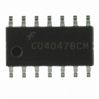
Manufacturer Part Number
CD4047BCMX
Description
MULTIVIBRATOR MONO/ASTABL 14SOIC
Manufacturer
Fairchild Semiconductor
Series
4000Br
Datasheet
1.CD4047BCMX.pdf
(9 pages)
Specifications of CD4047BCMX
Logic Type
Astable, Monostable
Independent Circuits
1
Schmitt Trigger Input
No
Propagation Delay
80ns
Current - Output High, Low
8.8mA, 8.8mA
Voltage - Supply
3 V ~ 15 V
Operating Temperature
-55°C ~ 125°C
Mounting Type
Surface Mount
Package / Case
14-SOIC (3.9mm Width), 14-SOL
Elements Per Chip
1
Logic Family
CD4000
Input Bias Current (max)
0.02 mA
Propagation Delay Time
1200 ns, 600 ns, 480 ns
High Level Output Current
- 4.2 mA
Low Level Output Current
4.2 mA
Supply Voltage (max)
15 V
Supply Voltage (min)
3 V
Maximum Power Dissipation
700 mW
Maximum Operating Temperature
+ 125 C
Minimum Operating Temperature
- 55 C
Mounting Style
SMD/SMT
Operating Supply Voltage
3.3 V, 5 V, 9 V, 12 V
Lead Free Status / RoHS Status
Lead free / RoHS Compliant
Other names
CD4047BCMX
CD4047BCMXTR
CD4047BCMXTR


© 2002 Fairchild Semiconductor Corporation
CD4047BCM
CD4047BCN
CD4047BC
Low Power Monostable/Astable Multivibrator
General Description
The CD4047B is capable of operating in either the
monostable or astable mode. It requires an external capac-
itor (between pins 1 and 3) and an external resistor
(between pins 2 and 3) to determine the output pulse width
in the monostable mode, and the output frequency in the
astable mode.
Astable operation is enabled by a high level on the astable
input or low level on the astable input. The output fre-
quency (at 50% duty cycle) at Q and Q outputs is deter-
mined by the timing components. A frequency twice that of
Q is available at the Oscillator Output; a 50% duty cycle is
not guaranteed.
Monostable operation is obtained when the device is trig-
gered by LOW-to-HIGH transition at
HIGH-to-LOW transition at
be retriggered by applying a simultaneous LOW-to-HIGH
transition to both the
A high level on Reset input resets the outputs Q to LOW, Q
to HIGH.
Features
Ordering Code:
Devices also available in Tape and Reel. Specify by appending the suffix letter “X” to the ordering code.
Order Number
Wide supply voltage range:
High noise immunity: 0.45 V
Low power TTL compatibility: Fan out of 2 driving 74L
or 1 driving 74LS
Special Features
Low power consumption: special CMOS oscillator
configuration
Monostable (one-shot) or astable (free-running)
operation
True and complemented buffered outputs
Only one external R and C required
Package Number
trigger and retrigger inputs.
M14A
N14A
trigger input. The device can
DD
3.0V to 15V
(typ.)
14-Lead Small Outline Integrated Circuit (SOIC), JEDEC MS-012, 0.150" Narrow
14-Lead Plastic Dual-In-Line Package (PDIP), JEDEC MS-001, 0.300" Wide
trigger input or
DS005969
Applications
• Frequency discriminators
• Timing circuits
• Time-delay applications
• Envelope detection
• Frequency multiplication
• Frequency division
Monostable Multivibrator
Features
Positive- or negative-edge trigger
Output pulse width independent of trigger pulse duration
Retriggerable option for pulse width expansion
Long pulse widths possible using small RC components
by means of external counter provision
Fast recovery time essentially independent of pulse
width
Pulse-width
approaching 100%
Astable Multivibrator Features
Free-running or gatable operating modes
50% duty cycle
Oscillator output available
Good astable frequency stability
typical
frequency
deviation (circuits trimmed to frequency V
10%)
Package Description
2%
0.5%
accuracy
0.03%/ C @ 100 kHz
0.015%/ C @ 10 kHz
maintained
October 1987
Revised March 2002
www.fairchildsemi.com
at
duty
DD
cycles
10V
Related parts for CD4047BCMX
Image
Part Number
Description
Manufacturer
Datasheet
Request
R

Part Number:
Description:
Low Power Monostable/Astable Multivibrator
Manufacturer:
Fairchild Semiconductor

Part Number:
Description:
Monostable Multivibrator Monostable Multivib
Manufacturer:
Fairchild Semiconductor
Datasheet:
Part Number:
Description:
Fairchild Semiconductor [IGBT MODULE]
Manufacturer:
Fairchild Semiconductor
Datasheet:

Part Number:
Description:
Discrete Semiconductor Modules
Manufacturer:
Fairchild Semiconductor
Part Number:
Description:
Discrete Semiconductor Modules
Manufacturer:
Fairchild Semiconductor
Part Number:
Description:
This N-Channel MOSFET is produced using Fairchild Semiconductor�s advanced Power Trench� process
Manufacturer:
Fairchild Semiconductor
Datasheet:
Part Number:
Description:
This N-Channel MOSFET is produced using Fairchild Semiconductor�s advanced Power Trench� process
Manufacturer:
Fairchild Semiconductor
Datasheet:
Part Number:
Description:
This N-Channel MOSFET is produced using Fairchild Semiconductor�s advanced PowerTrench� process
Manufacturer:
Fairchild Semiconductor
Datasheet:
Part Number:
Description:
This N-Channel MOSFET is produced using Fairchild Semiconductor�s advanced PowerTrench� process
Manufacturer:
Fairchild Semiconductor
Datasheet:
Part Number:
Description:
This N-Channel MOSFET is produced using Fairchild Semiconductor�s advanced Power Trench� process
Manufacturer:
Fairchild Semiconductor
Datasheet:
Part Number:
Description:
This N-Channel logic Level MOSFETs are produced using Fairchild Semiconductor�s advanced Power Trench� process that has been special tailored to minimize the on-state resistance and yet maintain superior switching performance
Manufacturer:
Fairchild Semiconductor
Datasheet:
Part Number:
Description:
This N-Channel MOSFET is produced using Fairchild Semiconductor�s advanced Power Trench� process
Manufacturer:
Fairchild Semiconductor
Datasheet:
Part Number:
Description:
This N-Channel SyncFET� is produced using Fairchild Semiconductor�s advanced PowerTrench� process
Manufacturer:
Fairchild Semiconductor
Datasheet:
Part Number:
Description:
This N-Channel SyncFET� is produced using Fairchild Semiconductor�s advanced PowerTrench� process
Manufacturer:
Fairchild Semiconductor
Datasheet: