MM74HC123AN Fairchild Semiconductor, MM74HC123AN Datasheet

IC MULTIVIBRATOR MONO DL 16-DIP

MM74HC123AN

Manufacturer Part Number
MM74HC123AN
Description
IC MULTIVIBRATOR MONO DL 16-DIP
Manufacturer
Fairchild Semiconductor
Series
74HCr
Datasheet

Specifications of MM74HC123AN

Logic Type
Monostable
Independent Circuits
2
Schmitt Trigger Input
Yes
Propagation Delay
22ns
Current - Output High, Low
5.2mA, 5.2mA
Voltage - Supply
2 V ~ 6 V
Operating Temperature
-40°C ~ 85°C
Mounting Type
Through Hole
Package / Case
16-DIP (0.300", 7.62mm)
Elements Per Chip
2
Logic Family
HC
Input Bias Current (max)
0.008 mA
Propagation Delay Time
197 ns, 48 ns, 38 ns
High Level Output Current
- 5.2 mA
Low Level Output Current
5.2 mA
Supply Voltage (max)
6 V
Supply Voltage (min)
2 V
Maximum Operating Temperature
+ 85 C
Minimum Operating Temperature
- 40 C
Mounting Style
Through Hole
Operating Supply Voltage
2.5 V, 3.3 V, 5 V
Lead Free Status / RoHS Status
Lead free / RoHS Compliant
Other names
74HC123
MM74HC123N

Available stocks

Company
Part Number
Manufacturer
Quantity
Price
Part Number:
MM74HC123AN
Manufacturer:
NS/国半
Quantity:
20 000
© 1999 Fairchild Semiconductor Corporation
MM74HC123AM
MM74HC123ASJ
MM74HC123AMTC
MM74HC123AN
MM74HC123A
Dual Retriggerable Monostable Multivibrator
General Description
The MM74HC123A high speed monostable multivibrators
(one shots) utilize advanced silicon-gate CMOS technol-
ogy. They feature speeds comparable to low power Schot-
tky TTL circuitry while retaining the low power and high
noise immunity characteristic of CMOS circuits.
Each multivibrator features both a negative, A, and a posi-
tive, B, transition triggered input, either of which can be
used as an inhibit input. Also included is a clear input that
when taken low resets the one shot. The MM74HC123A
can be triggered on the positive transition of the clear while
A is held LOW and B is held HIGH.
The MM74HC123A is retriggerable. That is it may be trig-
gered repeatedly while their outputs are generating a pulse
and the pulse will be extended.
Pulse width stability over a wide range of temperature and
supply is achieved using linear CMOS techniques. The out-
Ordering Code:
Devices also available in Tape and Reel. Specify by appending the suffix letter “X” to the ordering code.
Connection Diagram
Order Number
Pin Assignment for DIP, SOIC, SOP and TSSOP
Package Number
Top View
MTC16
M16A
M16D
N16E
16-Lead Small Outline Integrated Circuit (SOIC), JEDEC MS-012, 0.150” Narrow
16-Lead Small Outline Package (SOP), EIAJ TYPE II, 5.3mm Wide
16-Lead Thin Shrink Small Outline Package (TSSOP), JEDEC MO-153, 4.4mm Wide
16-Lead Plastic Dual-In-Line Package (PDIP), JEDEC MS-001, 0.300” Wide
DS005206.prf
put pulse equation is simply: PW
PW is in seconds, R is in ohms, and C is in farads. All
inputs are protected from damage due to static discharge
by diodes to V
Features
Note: Pin 6 and Pin 14 must be hard-wired to GND.
Typical propagation delay: 25 ns
Wide power supply range: 2V–6V
Low quiescent current: 80 A maximum (74HC Series)
Low input current: 1 A maximum
Fanout of 10 LS-TTL loads
Simple pulse width formula T
Wide pulse range: 400 ns to
Part to part variation: 5% (typ)
Schmitt Trigger A & B inputs enable infinite signal input
rise and fall times.
Package Description
CC
and ground.
Timing Component
September 1983
Revised February 1999
(typ)
RC
(R
EXT
www.fairchildsemi.com
) (C
EXT
); where

Related parts for MM74HC123AN

MM74HC123AN Summary of contents

Page 1

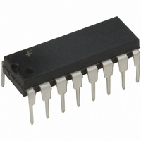
... MM74HC123AMTC MTC16 16-Lead Thin Shrink Small Outline Package (TSSOP), JEDEC MO-153, 4.4mm Wide MM74HC123AN N16E 16-Lead Plastic Dual-In-Line Package (PDIP), JEDEC MS-001, 0.300” Wide Devices also available in Tape and Reel. Specify by appending the suffix letter “X” to the ordering code. ...

Page 2

Truth Table Inputs Clear HIGH Level L LOW Level Transition from LOW-to-HIGH Transition from HIGH-to-LOW One HIGH Level Pulse One LOW Level Pulse X Irrelevant Logic Diagram www.fairchildsemi.com Outputs ...

Page 3

Absolute Maximum Ratings (Note 2) Supply Voltage ( Input Voltage ( Output Voltage ( OUT Clamp Diode Current ( Output Current, ...

Page 4

AC Electrical Characteristics Symbol Parameter t Maximum Trigger Propagation Delay PLH Clear Maximum Trigger Propagation Delay PHL ...

Page 5

Theory of Operation 1POSITIVE EDGE TRIGGER 2NEGATIVE EDGE TRIGGER 3POSITIVE EDGE TRIGGER 4POSITIVE EDGE RE-TRIGGER (PULSE LENGTHENING) 5RESET PULSE SHORTENING 6CLEAR TRIGGER TRIGGER OPERATION As shown in Figure 1 and the logic diagram, before an input trigger occurs, the one ...

Page 6

RESET OPERATION These one shots may be reset during the generation of the output pulse. In the reset mode of operation, an input pulse on clear sets the reset latch and causes the capacitor to be fast charged to V ...

Page 7

Physical Dimensions inches (millimeters) unless otherwise noted 16-Lead Small Outline Integrated Circuit (SOIC), JEDEC MS-012, 0.150” Narrow 16-Lead Small Outline Package (SOP), EIAJ TYPE II, 5.3mm Wide Package Number M16A Package Number M16D 7 www.fairchildsemi.com ...

Page 8

Physical Dimensions inches (millimeters) unless otherwise noted (Continued) 16-Lead Thin Shrink Small Outline Package (TSSOP), JEDEC MO-153, 4.4mm Wide www.fairchildsemi.com Package Number MTC16 8 ...

Page 9

Physical Dimensions inches (millimeters) unless otherwise noted (Continued) 16-Lead Plastic Dual-In-Line Package (PDIP), JEDEC MS-001, 0.300” Wide LIFE SUPPORT POLICY FAIRCHILD’S PRODUCTS ARE NOT AUTHORIZED FOR USE AS CRITICAL COMPONENTS IN LIFE SUPPORT DEVICES OR SYSTEMS WITHOUT THE EXPRESS WRITTEN ...

Related keywords