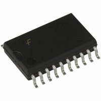
MM74HCT373WM Fairchild Semiconductor, MM74HCT373WM Datasheet - Page 6

MM74HCT373WM
Manufacturer Part Number
MM74HCT373WM
Description
IC LATCH OCTAL D 3 ST 20-SOICW
Manufacturer
Fairchild Semiconductor
Series
74HCTr
Type
D-Typer
Datasheet
1.MM74HCT374N.pdf
(10 pages)
Specifications of MM74HCT373WM
Logic Type
D-Type Transparent Latch
Circuit
8:8
Output Type
Tri-State
Voltage - Supply
4.5 V ~ 5.5 V
Independent Circuits
1
Delay Time - Propagation
25ns
Current - Output High, Low
7.2mA, 7.2mA
Operating Temperature
-40°C ~ 85°C
Mounting Type
Surface Mount
Package / Case
20-SOIC (7.5mm Width)
Logic Family
HCT
Number Of Bits
8
Number Of Elements
1
Latch Mode
Transparent
Polarity
Non-Inverting
Technology
CMOS
Package Type
SOIC W
Propagation Delay Time
56ns
Operating Supply Voltage (typ)
5V
High Level Output Current
-7.2mA
Low Level Output Current
7.2mA
Operating Supply Voltage (min)
4.5V
Operating Supply Voltage (max)
5.5V
Operating Temp Range
-40C to 85C
Operating Temperature Classification
Industrial
Mounting
Surface Mount
Pin Count
20
Latch Type
D Type
Output Current
7.2mA
Propagation Delay
30ns
No. Of Bits
8 Bit
Ic Output Type
Tri State
Supply Voltage Range
4.5V To 5.5V
Logic Case Style
SOIC
No. Of Pins
20
Rohs Compliant
Yes
Lead Free Status / RoHS Status
Lead free / RoHS Compliant
Available stocks
Company
Part Number
Manufacturer
Quantity
Price
Part Number:
MM74HCT373WM
Manufacturer:
FSC
Quantity:
20 000
Company:
Part Number:
MM74HCT373WMX
Manufacturer:
Fairchild Semiconductor
Quantity:
1 964
www.fairchildsemi.com
f
t
t
t
t
t
t
t
C
C
C
f
t
t
t
t
t
t
MAX
PHL
PZH
PHZ
THL
W
S
H
MAX
PHL
PZH
PHZ
W
S
H
Symbol
AC Electrical Characteristics
MM74HCT374: V
AC Electrical Characteristics
MM74HCT374: V
Note 6: C
IN
OUT
PD
, t
, t
, t
, t
, t
, t
, t
Symbol
TLH
PLH
PZL
PLZ
PLH
PZL
PLZ
PD
Maximum Clock Frequency
Maximum Propagation Delay
to Output
Maximum Enable Propagation
Delay Control to Output
Maximum Disable Propagation
Delay Control to Output
Maximum Output Rise
and Fall Time
Minimum Clock Pulse Width
Minimum Setup Time Data to Clock
Minimum Hold Time Clock to Data
Maximum Input Capacitance
Maximum Output Capacitance
Power Dissipation Capacitance
(Note 6)
determines the no load power consumption, P
CC
CC
Maximum Clock Frequency
Maximum Propagation Delay
to Output
Maximum Enable Propagation Delay
Control to Output
Maximum Disable Propagation Delay
Control to Output
Minimum Clock Pulse Width
Minimum Setup Time Data to Clock
Minimum Hold Time Clock to Data
Parameter
5.0V, t
5.0V
r
r
10%, t
Parameter
t
f
6 ns T
r
t
f
A
6 ns (unless otherwise specified)
C
C
C
C
R
C
R
OC
OC
C
25
L
L
L
L
L
L
L
L
q
C (unless otherwise specified)
50 pF
150 pF
50 pF
150 pF
1 k
50 pF
1 k
50 pF
V
GND
Conditions
D
CC
:
:
C
C
C
R
C
R
PD
L
L
L
L
L
V
45 pF
45 pF
1 k
5 pF
1 k
CC
2 f
:
:
Conditions
I
6
CC
V
CC
Typ
22
30
21
30
21
8
, and the no load dynamic current consumption, I
T
A
25
q
C
30
36
46
30
40
30
12
16
20
10
20
58
5
5
T
A
Guaranteed Limits
Typ
50
20
19
17
40 to 85
24
45
57
37
50
37
15
20
25
10
20
5
q
C T
Guaranteed
A
Limit
30
32
28
25
20
16
5
55 to 125
S
20
48
69
45
60
45
18
24
30
10
20
5
C
PD
V
q
CC
C
Units
f
MHz
ns
ns
ns
ns
ns
ns
Units
I
MHz
CC
pF
pF
pF
pF
ns
ns
ns
ns
ns
ns
ns
ns
ns
.


