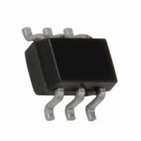
NC7WV14P6X Fairchild Semiconductor, NC7WV14P6X Datasheet - Page 3

NC7WV14P6X
Manufacturer Part Number
NC7WV14P6X
Description
IC INVERTER ULP-A DUAL SC70-6
Manufacturer
Fairchild Semiconductor
Series
7WVr
Specifications of NC7WV14P6X
Logic Type
Inverter
Number Of Inputs
1
Number Of Circuits
2
Current - Output High, Low
24mA, 24mA
Voltage - Supply
0.9 V ~ 3.6 V
Operating Temperature
-40°C ~ 85°C
Mounting Type
Surface Mount
Package / Case
SC-70-6, SC-88, SOT-363
Logic Family
NC7WV
High Level Output Current
- 24 mA
Low Level Output Current
24 mA
Supply Voltage (max)
3.6 V
Supply Voltage (min)
0.9 V
Maximum Operating Temperature
+ 85 C
Minimum Operating Temperature
- 40 C
Mounting Style
SMD/SMT
Operating Supply Voltage
3 V to 3.6 V
Logical Function
Inverter Schmit Trig
Number Of Elements
2
Input Type
Schmitt Trigger
Propagation Delay Time
15.6ns
Operating Supply Voltage (typ)
1.8/2.5/3.3V
Package Type
SC-70
Operating Temp Range
-40C to 85C
Pin Count
6
Quiescent Current
900nA
Output Type
Schmitt Trigger
Technology
CMOS
Mounting
Surface Mount
Operating Temperature Classification
Industrial
Operating Supply Voltage (max)
3.6V
Operating Supply Voltage (min)
0.9V
Lead Free Status / RoHS Status
Lead free / RoHS Compliant
Available stocks
Company
Part Number
Manufacturer
Quantity
Price
©2003 Fairchild Semiconductor Corporation
NC7WV14 Rev. 1.0.0
Absolute Maximum Ratings
Stresses exceeding the absolute maximum ratings may damage the device. The device may not function or be
operable above the recommended operating conditions and stressing the parts to these levels is not recommended.
In addition, extended exposure to stresses above the recommended operating conditions may affect device reliability.
The absolute maximum ratings are stress ratings only.
Recommended Operating Conditions
The Recommended Operating Conditions table defines the conditions for actual device operation. Recommended
operating conditions are specified to ensure optimal performance to the datasheet specifications. Fairchild does not
recommend exceeding them or designing to absolute maximum ratings.
Notes:
1. I
2. Unused inputs must be held HIGH or LOW. They may not float.
I
CC
Symbol
I
O
OH
Symbol
V
I
V
t / V
V
Absolute Maximum Rating must be observed.
OH
or Ground
OUT
T
V
T
CC
JA
V
IN
/ I
V
A
I
P
OUT
I
STG
T
T
OK
CC
IK
OL
IN
/ I
D
J
L
OL
Supply Voltage
Input Voltage
Output Voltage
Output Current in I
Free Air Operating Temperature
Minimum Input Edge Rate @ V
Thermal Resistance
HIGH or LOW State
V
V
V
V
V
V
V
SC70-6
Micropak-6
Supply Voltage
DC Input Voltage
DC Output Voltage
DC Input Diode Current @ V
DC Output Diode Current
DC Output Source/Sink Current
DC V
Storage Temperature Range
Junction Temperature Under Bias
Junction Lead Temperature (Soldering, 10 seconds)
Power Dissipation @ +85°C
CC
CC
CC
CC
CC
CC
CC
HIGH or LOW State
V
V
V
SC70-6
Micropak-6
OUT
OUT
CC
CC
0V
3.0V to 3.6V
2.3V to 2.7V
1.65V to 1.95V
1.4V to 1.6V
1.1V to 1.3V
0.9V
or Ground Current per Supply Pin
0V
V
0V
CC
OH
/ I
OL
(1)
Parameter
IN
Parameter
IN
0.8V to 2.0V, V
0V
(2)
3
CC
3.0V
–0.5V to V
Rating
Rating
–65°C to +150°C
–40°C to +85°C
–0.5V to +4.6V
–0.5V to +4.6V
–0.5V to +4.6V
www.fairchildsemi.com
0.9V to 3.6V
0V to 3.6V
0V to 3.6V
0V to V
CC
350°C/W
310°C/W
185mW
210mW
±0.1mA
+50mA
±50mA
±50mA
±24mA
±18mA
–50mA
–50mA
10ns/V
150°C
260°C
+0.5V
±6mA
±4mA
±2mA
CC


