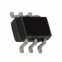
NC7SZ175P6 Fairchild Semiconductor, NC7SZ175P6 Datasheet - Page 3

NC7SZ175P6
Manufacturer Part Number
NC7SZ175P6
Description
IC FLIP FLOP UHS D-TYPE SC70-6
Manufacturer
Fairchild Semiconductor
Series
7SZr
Type
D-Typer
Datasheet
1.NC7SZ175P6X.pdf
(9 pages)
Specifications of NC7SZ175P6
Function
Reset
Output Type
Differential
Number Of Elements
1
Number Of Bits Per Element
1
Frequency - Clock
100MHz
Delay Time - Propagation
9.8ns
Trigger Type
Positive Edge
Current - Output High, Low
32mA, 32mA
Voltage - Supply
1.65 V ~ 5.5 V
Operating Temperature
-40°C ~ 85°C
Mounting Type
Surface Mount
Package / Case
SC-70-6, SC-88, SOT-363
Package
6SC-70
Logic Function
D-Type
Logic Family
TinyLogic UHS
Number Of Elements Per Chip
1
Output Signal Type
Single-Ended
Set/reset
Master Reset
Typical Operating Supply Voltage
1.8|2.5|3.3|5 V
Lead Free Status / RoHS Status
Lead free / RoHS Compliant
Other names
NC7SZ175P6TR
Available stocks
Company
Part Number
Manufacturer
Quantity
Price
Company:
Part Number:
NC7SZ175P6
Manufacturer:
FSC
Quantity:
1 500
Company:
Part Number:
NC7SZ175P6X
Manufacturer:
FSC
Quantity:
500
Company:
Part Number:
NC7SZ175P6X
Manufacturer:
Fairchild Semiconductor
Quantity:
168 075
Part Number:
NC7SZ175P6X
Manufacturer:
FAIRCHILD/仙童
Quantity:
20 000
V
V
V
V
I
I
I
IN
OFF
CC
Symbol
Absolute Maximum Ratings
DC Electrical Characteristics
IH
IL
OH
OL
Supply Voltage (V
DC Input Voltage (V
DC Output Voltage (V
DC Input Diode Current (I
DC Output Diode Current (I
DC Output (I
DC V
Storage Temperature Range (T
Junction Temperature under Bias (T
Junction Lead Temperature (T
Power Dissipation (P
V
V
(Soldering, 10 seconds)
IN
OUT
CC
/GND Current (I
0V
HIGH Level Control
Input Voltage
LOW Level Control
Input Voltage
HIGH Level Control
Output Voltage
LOW Level Control
Output Voltage
Input Leakage Current
Power Off Leakage Current
Quiescent Supply Current
0V
OUT
) Source/Sink Current
Parameter
CC
IN
)
D
)
OUT
) @ 85 C
CC
)
IK
/I
)
OK
GND
)
L
STG
)
)
)
J
)
1.65 to 1.95 0.75 V
1.65 to 1.95
1.65 to 5.5
2.3 to 5.5
2.3 to 5.5
0 to 5.5
1.65
1.65
1.65
1.65
V
(V)
1.8
2.3
3.0
4.5
2.3
3.0
3.0
4.5
1.8
2.3
3.0
4.5
2.3
3.0
3.0
4.5
0.0
CC
65 C to 150 C
0.5V to 7.0V
0.5V to 7.0V
0.5V to 7.0V
(Note 1)
0.7 V
180 mW
1.55
1.24
Min
1.7
2.2
2.9
4.4
1.9
2.4
2.3
3.8
50 mA
50 mA
50 mA
50 mA
150 C
260 C
CC
CC
T
A
1.65
1.52
2.15
2.68
0.08
0.10
0.15
0.22
0.22
3
Typ
1.8
2.3
3.0
4.5
2.8
4.2
0.0
0.0
0.0
0.0
0.0
Recommended Operating
Conditions
Note 1: The “Absolute Maximum Ratings”: are those values beyond which
the safety of the device cannot be guaranteed. The device should not be
operated at these limits. The parametric values defined in the Electrical
Characteristics tables are not guaranteed at the absolute maximum ratings.
The “Recommended Operating Conditions” table will define the conditions
for actual device operation.
Note 2: Unused inputs must be held HIGH or LOW. They may not float.
25 C
Power Supply
Input Voltage (V
Output Voltage (V
Input Rise and Fall Time (t
Operating Temperature (T
Thermal Resistance (
Operating (V
Data Retention
V
V
V
CC
CC
CC
0.25 V
0.3 V
Max
0.24
0.55
0.55
0.1
0.1
0.1
0.1
0.1
0.3
0.4
1.0
1.0
0.1
1.8V, 2.5V
3.3V
5.5V
CC
CC
T
0.75 V
0.7 V
CC
A
0.3V
0.5V
IN
1.55
1.29
Min
1.7
2.2
2.9
4.4
1.9
2.4
2.3
3.8
)
)
OUT
(Note 2)
CC
40 C to 85 C
CC
)
0.2V
JA
0.25 V
0.3 V
)
A
Max
0.24
0.55
0.55
10.0
r
0.1
0.1
0.1
0.1
0.1
0.3
0.4
10
, t
)
1.0
f
CC
)
CC
Unit
V
V
V
V
A
A
A
www.fairchildsemi.com
V
or V
V
or V
0
V
V
IN
IN
IN
IN
V
or V
IL
IH
IN
V
V
5.5V, GND
40 C to 85 C
Conditions
1.65V to 5.5V
IH
IL
OUT
1.5V to 5.5V
0 to 20 ns/V
0 to 10 ns/V
5.5V
0 to 5 ns/V
0V to 5.5V
I
I
I
I
I
I
I
I
I
I
I
I
0V to V
350 C/W
OH
OH
OH
OH
OH
OH
OL
OL
OL
OL
OL
OL
5.5V
100 A
4 mA
8 mA
16 mA
24 mA
32 mA
100 A
4 mA
8 mA
16 mA
24 mA
32 mA
CC


