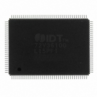
IDT72V36100L15PFI IDT, Integrated Device Technology Inc, IDT72V36100L15PFI Datasheet - Page 41

IDT72V36100L15PFI
Manufacturer Part Number
IDT72V36100L15PFI
Description
IC FIFO SYNC II 36BIT 128-TQFP
Manufacturer
IDT, Integrated Device Technology Inc
Series
72Vr
Datasheet
1.IDT72V36110L7-5BB.pdf
(48 pages)
Specifications of IDT72V36100L15PFI
Function
Synchronous
Memory Size
2.3K (64 x 36)
Data Rate
166MHz
Access Time
15ns
Voltage - Supply
3.15 V ~ 3.45 V
Operating Temperature
-40°C ~ 85°C
Mounting Type
Surface Mount
Package / Case
128-TQFP, 128-VQFP
Configuration
Dual
Density
2.25Mb
Access Time (max)
10ns
Word Size
36b
Organization
64Kx36
Sync/async
Synchronous
Expandable
Yes
Bus Direction
Uni-Directional
Package Type
TQFP
Clock Freq (max)
66.7MHz
Operating Supply Voltage (typ)
3.3V
Operating Supply Voltage (min)
3.15V
Operating Supply Voltage (max)
3.45V
Supply Current
40mA
Operating Temp Range
-40C to 85C
Operating Temperature Classification
Industrial
Mounting
Surface Mount
Pin Count
128
Lead Free Status / RoHS Status
Contains lead / RoHS non-compliant
Other names
72V36100L15PFI
800-1529
800-1529
Available stocks
Company
Part Number
Manufacturer
Quantity
Price
Company:
Part Number:
IDT72V36100L15PFI
Manufacturer:
IDT, Integrated Device Technology Inc
Quantity:
10 000
Company:
Part Number:
IDT72V36100L15PFI8
Manufacturer:
IDT, Integrated Device Technology Inc
Quantity:
10 000
OPTIONAL CONFIGURATIONS
WIDTH EXPANSION CONFIGURATION
signals of multiple devices. Status flags can be detected from any one device.
The exceptions are the EF and FF functions in IDT Standard mode and the IR
and OR functions in FWFT mode. Because of variations in skew between RCLK
and WCLK, it is possible for EF/FF deassertion and IR/OR assertion to vary
NOTES:
1. Use an AND gate in IDT Standard mode, an OR gate in FWFT mode.
2. Do not connect any output control signals directly together.
3. FIFO #1 and FIFO #2 must be the same depth, but may be different word widths.
IDT72V36100/72V36110 3.3V HIGH DENSITY SUPERSYNC II
65,536 x 36 and 131,072 x 36
Word width may be increased simply by connecting together the control
GATE
FIRST WORD FALL THROUGH/
(1)
DATA IN
SERIAL INPUT (FWFT/SI)
PARTIAL RESET (PRS)
MASTER RESET (MRS)
FULL FLAG/INPUT READY (FF/IR)
FULL FLAG/INPUT READY (FF/IR) #2
RETRANSMIT (RT)
m + n
PROGRAMMABLE (PAF)
WRITE CLOCK (WCLK)
WRITE ENABLE (WEN)
HALF-FULL FLAG (HF)
Figure 29. Block Diagram of 65,536 x 72 and 131,072 x 72 Width Expansion
D
0
- Dm
LOAD (LD)
m
#1
72V36100
72V36110
FIFO
IDT
#1
TM
36-BIT FIFO
Dm
m
+1
- Dn
Q
41
0
n
- Qm
by one cycle between FIFOs. In IDT Standard mode, such problems can be
avoided by creating composite flags, that is, ANDing EF of every FIFO, and
separately ANDing FF of every FIFO. In FWFT mode, composite flags can be
created by ORing OR of every FIFO, and separately ORing IR of every FIFO.
72V36110 devices. D
Q
be attained by adding additional IDT72V36100/72V36110 devices.
0
-Q
Figure 29 demonstrates a width expansion using two IDT72V36100/
72V36100
72V36110
35
FIFO
IDT
#2
from each device form a 72-bit wide output bus. Any word width can
READ CLOCK (RCLK)
n
READ ENABLE (REN)
OUTPUT ENABLE (OE)
EMPTY FLAG/OUTPUT READY (EF/OR) #2
EMPTY FLAG/OUTPUT READY (EF/OR) #1
PROGRAMMABLE (PAE)
Qm
0
- D
+1
35
- Qn
from each device form a 72-bit wide input bus and
COMMERCIAL AND INDUSTRIAL
m + n
TEMPERATURE RANGES
DATA OUT
OCTOBER 22, 2008
6117 drw34
GATE
(1)


