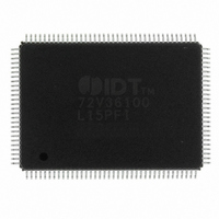
IDT72V36100L15PFI IDT, Integrated Device Technology Inc, IDT72V36100L15PFI Datasheet - Page 35

IDT72V36100L15PFI
Manufacturer Part Number
IDT72V36100L15PFI
Description
IC FIFO SYNC II 36BIT 128-TQFP
Manufacturer
IDT, Integrated Device Technology Inc
Series
72Vr
Datasheet
1.IDT72V36110L7-5BB.pdf
(48 pages)
Specifications of IDT72V36100L15PFI
Function
Synchronous
Memory Size
2.3K (64 x 36)
Data Rate
166MHz
Access Time
15ns
Voltage - Supply
3.15 V ~ 3.45 V
Operating Temperature
-40°C ~ 85°C
Mounting Type
Surface Mount
Package / Case
128-TQFP, 128-VQFP
Configuration
Dual
Density
2.25Mb
Access Time (max)
10ns
Word Size
36b
Organization
64Kx36
Sync/async
Synchronous
Expandable
Yes
Bus Direction
Uni-Directional
Package Type
TQFP
Clock Freq (max)
66.7MHz
Operating Supply Voltage (typ)
3.3V
Operating Supply Voltage (min)
3.15V
Operating Supply Voltage (max)
3.45V
Supply Current
40mA
Operating Temp Range
-40C to 85C
Operating Temperature Classification
Industrial
Mounting
Surface Mount
Pin Count
128
Lead Free Status / RoHS Status
Contains lead / RoHS non-compliant
Other names
72V36100L15PFI
800-1529
800-1529
Available stocks
Company
Part Number
Manufacturer
Quantity
Price
Company:
Part Number:
IDT72V36100L15PFI
Manufacturer:
IDT, Integrated Device Technology Inc
Quantity:
10 000
Company:
Part Number:
IDT72V36100L15PFI8
Manufacturer:
IDT, Integrated Device Technology Inc
Quantity:
10 000
NOTE:
1. This timing diagram illustrates programming with an input bus width of 36 bits.
NOTES:
1. OE = LOW.
2. The timing diagram illustrates reading of offset registers with an output bus width of 36 bits.
D
Q
WCLK
RCLK
NOTES:
1. m = PAF offset.
2. D = maximum FIFO depth.
3. t
4. PAF is asserted and updated on the rising edge of WCLK only.
5. Select this mode by setting PFM HIGH during Master Reset.
IDT72V36100/72V36110 3.3V HIGH DENSITY SUPERSYNC II
65,536 x 36 and 131,072 x 36
WCLK
RCLK
WEN
0
REN
0
PAF
WEN
In IDT Standard mode: D = 65,536 for the IDT72V36100 and 131,072 for the IDT72V36110.
In FWFT mode: D = 65,537 for the IDT72V36100 and 131,073 for the IDT72V36110.
rising edge of RCLK and the rising edge of WCLK is less than t
REN
SKEW2
- D
- Q
LD
LD
n
n
is the minimum time between a rising RCLK edge and a rising WCLK edge to guarantee that PAF will go HIGH (after one WCLK cycle plus t
t
CLKL
Figure 18. Synchronous Programmable Almost-Full Flag Timing (IDT Standard and FWFT Modes)
t
Figure 16. Parallel Loading of Programmable Flag Registers (IDT Standard and FWFT Modes)
ENS
Figure 17. Parallel Read of Programmable Flag Registers (IDT Standard and FWFT Modes)
D - (m+1) words in FIFO
t
CLKL
DATA IN OUTPUT REGISTER
t
ENH
t
CLKH
t
CLKH
1
(2)
t
CLK
t
CLK
SKEW2
t
t
ENS
LDS
t
t
CLKL
DS
t
, then the PAF deassertion time may be delayed one extra WCLK cycle.
TM
t
ENS
LDS
t
CLKL
36-BIT FIFO
OFFSET
PAE
2
t
PAFS
35
t
t
t
ENH
DH
LDH
t
LDH
t
t
t
ENH
A
ENS
t
SKEW2
(3)
OFFSET
PAF
PAE OFFSET
t
ENH
D - m words in FIFO
t
1
t
t
DH
LDH
ENH
t
t
ENH
LDH
t
A
COMMERCIAL AND INDUSTRIAL
(2)
2
TEMPERATURE RANGES
PAFS
t
PAFS
OCTOBER 22, 2008
PAF OFFSET
). If the time between the
D-(m+1) words
in FIFO
6117 drw 23
6117 drw 21
6117 drw 22
(2)


