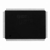
IDT72V36110L10PF IDT, Integrated Device Technology Inc, IDT72V36110L10PF Datasheet - Page 3

IDT72V36110L10PF
Manufacturer Part Number
IDT72V36110L10PF
Description
IC FIFO SYNC 131KX36 10NS 128QFP
Manufacturer
IDT, Integrated Device Technology Inc
Series
72Vr
Datasheet
1.IDT72V36110L7-5BB.pdf
(48 pages)
Specifications of IDT72V36110L10PF
Function
Synchronous
Memory Size
4.7M (131K x 36)
Data Rate
166MHz
Access Time
10ns
Voltage - Supply
3.15 V ~ 3.45 V
Operating Temperature
0°C ~ 70°C
Mounting Type
Surface Mount
Package / Case
128-TQFP, 128-VQFP
Configuration
Dual
Density
4.5Mb
Access Time (max)
6.5ns
Word Size
36b
Organization
128Kx36
Sync/async
Synchronous
Expandable
Yes
Bus Direction
Uni-Directional
Package Type
TQFP
Clock Freq (max)
100MHz
Operating Supply Voltage (typ)
3.3V
Operating Supply Voltage (min)
3.15V
Operating Supply Voltage (max)
3.45V
Supply Current
40mA
Operating Temp Range
0C to 70C
Operating Temperature Classification
Commercial
Mounting
Surface Mount
Pin Count
128
Lead Free Status / RoHS Status
Contains lead / RoHS non-compliant
Other names
72V36110L10PF
800-1530
800-1530
Available stocks
Company
Part Number
Manufacturer
Quantity
Price
Company:
Part Number:
IDT72V36110L10PF
Manufacturer:
IDT, Integrated Device Technology Inc
Quantity:
10 000
Part Number:
IDT72V36110L10PF
Manufacturer:
IDT
Quantity:
20 000
Company:
Part Number:
IDT72V36110L10PF8
Manufacturer:
IDT, Integrated Device Technology Inc
Quantity:
10 000
WCLK when WEN is asserted. During Asynchronous operation only the WR
input is used to write data into the FIFO. Data is written on a rising edge of WR,
the WEN input should be tied to its active state, (LOW).
or Asynchronous interface. During Synchronous operation the output port is
controlled by a Read Clock (RCLK) input and Read Enable (REN) input. Data
is read from the FIFO on every rising edge of RCLK when REN is asserted.
During Asynchronous operation only the RD input is used to read data from the
FIFO. Data is read on a rising edge of RD, the REN input should be tied to its
PIN CONFIGURATIONS (CONTINUED)
DESCRIPTION (CONTINUED)
IDT72V36100/72V36110 3.3V HIGH DENSITY SUPERSYNC II
65,536 x 36 and 131,072 x 36
The output port can be selected as either a Synchronous (clocked) interface,
A
B
C
D
F
H
K
L
E
G
J
M
ASYW
SEN
D32
D26
D10
D21
D12
D35
D29
D18
D15
D9
1
WEN
D34
D31
D25
D11
D22
D19
D16
IW
D28
D13
D8
2
A1 BALL PAD CORNER
WCLK
PRS
D27
D33
D30
D24
D20
D23
D14
D17
D6
D7
3
FWFT/SI
PBGA: 1mm pitch, 13mm x 13mm (BB144-1, order code: BB)
V
V
V
V
PAF
V
V
D4
LD
D5
4
CC
CC
CC
CC
D3
CC
CC
FF/IR
MRS
GND
GND
GND
GND
V
OW
V
D0
D1
D2
5
CC
CC
TM
36-BIT FIFO
GND
TRST
GND
GND
GND
GND
GND
TMS
FS0
V
V
HF
CC
CC
6
TOP VIEW
3
active state, LOW. When Asynchronous operation is selected on the output port
the FIFO must be configured for Standard IDT mode, and the OE input used
to provide three-state control of the outputs, Qn.
to f
of the one clock input with respect to the other.
Standard mode and First Word Fall Through (FWFT) mode.
on the data output lines unless a specific read operation is performed. A read
GND
GND
GND
GND
GND
GND
TCK
V
V
FS1
BM
TDI
MAX
The frequencies of both the RCLK and the WCLK signals may vary from 0
In IDT Standard mode, the first word written to an empty FIFO will not appear
CC
CC
There are two possible timing modes of operation with these devices: IDT
7
with complete independence. There are no restrictions on the frequency
ASYR
GND
GND
GND
GND
TDO
V
V
BE
Q0
Q1
EF
CC
CC
8
RCLK
PAE
V
V
V
V
V
V
Q2
Q3
Q4
IP
CC
CC
CC
CC
CC
9
CC
PFM
REN
Q29
Q16
RM
Q26
Q23
Q19
Q13
Q22
Q5
Q6
10
COMMERCIAL AND INDUSTRIAL
Q15
Q10
Q32
Q30
Q24
Q21
Q18
Q12
Q27
Q7
11
OE
RT
TEMPERATURE RANGES
6117 drw02b
Q35
Q34
Q31
Q25
Q20
Q17
Q11
OCTOBER 22, 2008
Q28
Q14
Q8
Q3
Q9
3
12


